MAHA SET 2026 Paper II Electronic Science Set A Question Paper
Finished viewing? Save it for later —
Download MAHA SET 2026 Paper II Electronic Science Set A Question Paper (PDF · 20 pages)About MAHA SET 2026 Paper II Electronic Science Set A Question Paper
MAHA SET 2026 Paper II Electronic Science Set A Question Paper is available here for free download. Published by Maharashtra Exams for MAHA SET, this question paper can be viewed online or downloaded as a PDF (20 pages). Candidates preparing for MAHA SET can use MAHA SET 2026 Paper II Electronic Science Set A Question Paper to understand the exam pattern, the type of questions asked, and the overall difficulty level.
Frequently Asked Questions
How can I download MAHA SET 2026 Paper II Electronic Science Set A Question Paper?
Open this page and click the Download button to save MAHA SET 2026 Paper II Electronic Science Set A Question Paper as a PDF. It is completely free on AglaSem Docs.
Is MAHA SET 2026 Paper II Electronic Science Set A Question Paper free to download?
Yes. MAHA SET 2026 Paper II Electronic Science Set A Question Paper can be viewed online and downloaded as a PDF free of cost on AglaSem Docs.
How many pages does MAHA SET 2026 Paper II Electronic Science Set A Question Paper have?
MAHA SET 2026 Paper II Electronic Science Set A Question Paper contains 20 pages, which you can read online or download together as a single PDF.
Where can I find more MAHA SET study material?
You can find more MAHA SET question papers, sample papers, syllabus, and answer keys on AglaSem Docs.
MAHA SET 2026 Paper II Electronic Science Set A Question Paper – Text
Read the full text of this question paper below — useful to quickly search, copy and reference the content online without downloading the PDF.
📄 View text version (21 pages)
Page 1
MAHA SET 2026 Paper
II Electronic Science Set
A Question Paper
EXAM YEAR TYPE
MAHA SET 2026 Question Paper
Notes · Sample Papers · Previous Year Papers · Mock Tests
Page 2
. s e
em l a
as
a g
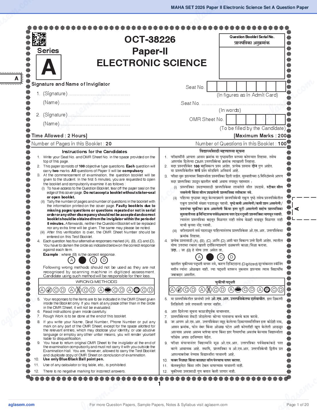
OCT-38226 Question Booklet Serial No.
àíZn{ÌH$m AZwH«$_m§H$>
Series Paper-II
ΔΔΔΔΔΔΔΔΔΔΔΔΔ A ELECTRONIC SCIENCE
m
ΔΔΔΔΔΔ
A
om co
Signature and Name of Invigilator
.
ΔΔΔΔΔΔΔΔΔΔΔΔ
Seat No.
.c e m
1. (Signature) ............................................. (In figures as in Admit Card)
e m
(Name) ...................................................
l a s
Seat No. ..............................................................
l a s (In words)
a g
ag
2. (Signature) .............................................
OMR Sheet No.
(Name) ...................................................
(To be filled by the Candidate)
Time Allowed : 2 Hours] [Maximum Marks : 200
Number of Pages in this Booklet : 20 Number of Questions in this Booklet : 100
Instructions for the Candidates {dÚmÏ`mªgmR>r _hÎdmÀ`m gyMZm
1. Write your Seat No. and OMR Sheet No. in the space provided on the 1.narjmWvZr Amnbm AmgZ H«$_m§H$ `m n¥îR>mdarb daÀ`m H$monè`mV {bhmdm. VgoM
top of this page. AmnUm§g {Xboë`m OMR CÎman{ÌHo$Mm H«$_m§H$ Ë`mImbr {bhmdm.
2. This paper consists of 100 objective type questions. Each question will 2. gXa àíZn{ÌHo$V 100 ~hþ{dH$ën àíZ AmhoV. àË`oH$ àíZmg XmoZ JwU AmhoV.
carry two marks. All questions of Paper II will be compulsory. `m àíZn{ÌHo$Vrb gd© àíZ gmoS>{dUo A{Zdm`© Amho.
3. At the commencement of examination, the question booklet will be 3. narjm gwê$ Pmë`mda {dÚmÏ`m©bm àíZn{ÌH$m {Xbr OmB©b. gwédmVrÀ`m 5 {_{ZQ>m_
§ Ü`o AmnU
m
given to the student. In the first 5 minutes, you are requested to open
co
the booklet and compulsorily examine it as follows :
gXa àíZn{ÌH$m CKSy>Z Imbrb ~m~r Adí` VnmgyZ nhmì`mV :
.
(i) To have access to the Question Booklet, tear off the paper seal on the (i) àíZn{ÌH$m CKS>Ê`mgmR>r àíZn{ÌHo$da bmdbobo grb CKS>mdo. ñQ>rH$a grb
em
edge of this cover page. Do not accept a booklet without sticker-seal Zgbobr {H§$dm grb CKS>bobr àíZn{ÌH$m ñdrH$mê$ Z`o.
or open booklet.
s
(ii) n{hë`m n¥îR>mda Z_yX Ho$ë`mà_mUo àíZn{ÌHo$Mr EHy$U n¥îR>o VgoM àíZn{ÌHo$Vrb
a
(ii) Tally the number of pages and number of questions in the booklet with
l
EHy$U àíZm§Mr g§»`m nS>VmiyZ nhmdr. n¥îR>o H$_r Agbobr/H$_r àíZ Agbobr/
the information printed on the cover page. Faulty booklets due to
g
A
missing pages/questions or questions repeated or not in serial àíZm§Mm MwH$sMm H«$_ Agbobr {H§$dm BVa ÌwQ>r Agbobr gXmof àíZn{ÌH$m
a
order or any other discrepancy should not be accepted and correct gwédmVrÀ`m 5 {_{ZQ>mVM n`©dojH$mbm naV XoD$Z Xwgar àíZn{ÌH$m _mJdyZ ¿`mdr.
booklet should be obtained from the invigilator within the period of Ë`mZ§Va àíZn{ÌH$m ~XbyZ {_iUma Zmhr VgoM doihr dmT>dyZ {_iUma Zmhr
5 minutes. Afterwards, neither the Question Booklet will be replaced `mMr H¥$n`m Zm|X ¿`mdr.
nor any extra time will be given. The same may please be noted.
(iii) After this verification is over, the OMR Sheet Number should be (iii) darbà_mUo gd© nS>VmiyZ nm{hë`mZ§VaM àíZn{ÌHo$da Amo.E_.Ama. CÎman{ÌHo$Mm
entered on this Test Booklet. H«$_m§H$ {bhmdm.
4. Each question has four alternative responses marked (A), (B), (C) and (D). 4. àË`oH$ àíZmgmR>r (A), (B), (C) Am{U (D) Aer Mma {dH$ën CÎmao {Xbr AmhoV. Ë`mVrb
You have to darken the circle as indicated below on the correct response `mo½` CÎmamMm aH$mZm Imbr Xe©{dë`mà_mUo R>iH$nUo H$mim/{Zim H$amdm.
against each item. CXm. : Oa (B) ho `mo½` CÎma Agob Va.
Example : where (B) is the correct response.
A B C D
A B C D
Imbrb MwH$sÀ`m nX²²YVr dmnê$ Z`o, H$maU {S>{OQ>mBÁS> (Digitized) _yë`m§H$ZmV ñH°${Z§J
Following wrong methods should not be used as they are not
_erZ Ë`m§Zm AmoiIV Zmhr. Ë`m nX²YVr dmnê$Z ZwH$gmZ Pmë`mg Ë`mg {dÚmWuM
m
recognised by scanning machine in digitized assessment.
c. o
Candidate using such method will be responsible for their loss. O~m~Xma AgVrb.
m
wrong methods MwH$sMr nX²²YVr
c. o e m
A
B C D A B C D A B C D A B C D A
B C D A B C D A B C D A B C D
em
5. Your responses to the items are to be indicated in the OMR Sheet given 5.
la s
`m àíZn{ÌHo$Vrb àíZm§Mr CÎmao Amo.E_.Ama. CÎman{ÌHo$VM Xe©dmdrV. BVa {R>H$mUr
las ag
inside the Booklet only. If you mark at any place other than in the circle {b{hbobr CÎmao Vnmgbr OmUma ZmhrV.
in the OMR Sheet, it will not be evaluated.
g
6. Read instructions given inside carefully. 6.AmV {Xboë`m gyMZm H$miOrnyd©H$ dmMmì`mV.
a
7. Rough Work is to be done at the end of this booklet. 7.àíZn{ÌHo$À`m eodQ>r OmoS>boë`m H$moè`m nmZmdaM H$ÀMo H$m_ H$amdo.
8. If you write your Name, Seat Number, Phone Number or put any 8.Oa AmnU Amo.E_.Ama. CÎman{ÌHo$da Z_yX Ho$boë`m {R>H$mUmì`{V{aŠV BVa H$moR>ohr Zmd,
mark on any part of the OMR Sheet, except for the space allotted for AmgZ H«$_m§H$, \$moZ Z§~a {H§$dm AmoiI nQ>ob Aer H$moUVrhr IyU Ho$bobr AmT>iyZ
the relevant entries, which may disclose your identity, or use abusive
language or employ any other unfair means, you will render yourself
Amë`mg AWdm Agä` ^mfoMm dmna {H§$dm BVa J¡a_mJmªMm Adb§~ Ho$ë`mg {dÚmÏ`m©bm
liable to disqualification. narjog AnmÌ R>a{dÊ`mV `oB©b.
9. You have to return original OMR Sheet to the invigilator at the end of 9. narjm g§në`mZ§Va {dÚmÏ`m©Zo _yi Amo.E_.Ama. CÎman{ÌH$m n`©dojH$m§H$S>o naV
the examination compulsorily and must not carry it with you outside the
Examination Hall. You are, however, allowed to carry the Test Booklet
H$aUo Amdí`H$ Amho. VWm{n, àíZn{ÌH$m d Amo.E_.Ama. CÎman{ÌHo$Mr {ÛVr` àV
and duplicate copy of OMR Sheet on conclusion of examination. Amnë`m~amo~a ZoÊ`mg {dÚmÏ`mªZm nadmZJr Amho.
10. Use only Blue/Black Ball point pen. 10. \$ŠV {Ziçm {H§$dm H$miçm ~m°b noZMmM dmna H$amdm.
11. Use of any calculator or log table, etc., is prohibited. 11. H°$bŠ`wboQ>a {H§$dm bm°J Q>o~b dmnaÊ`mg nadmZJr Zmhr.
c
12. There is no negative marking for incorrect answers. 12. MwH$sÀ`m CÎmamgmR>r JwU H$nmV Ho$br OmUma Zmhr.
m .
c. o
e m
1
m a s
se
For more Question Papers, Sample Papers, Notes & Syllabus visit
g l Page 1 of 20
Page 3
For more Question Papers, Sample Papers, Notes & Syllabus visit Page 2 of 20
Page 4
. s e
em l a
as a g
Electronic Science
Paper II
m
co
Time Allowed : 120 Minutes] [Maximum Marks : 200
c om m .
Note : This Paper contains Hundred (100) multiple choice questions. Each question
m .
carrying Two (2) marks. Attempt All questions.
s e
s e g l a
g l a a
theathreshold voltage is
1. For enhancement mode n-MOSFET, 4. Aluminium has been discarded as gate
metal in MOSFET because
(A) Equal to 0
(A) It is difficult to deposit Al
(B) Greater than zero or positive
quantity (B) Al has a lower conductivity than
(C) Negative voltage or lesser than polysilicon
zero
(C) Al gets easily oxidised
m cannot withstand high
(D) Determined by applied gate
c. o (D) Altemperature
voltage
e m
l a
2. Stick diagrams are those which convey s
layer information through
(A) thickness a g 5. Oxidation process in silicon planar
technology is also called as
(B) color (A) Photo oxidation
(C) shapes
(B) Encapsulation
(D) layers
(C) Vapour oxidation
3. What is the design flow of VLSI system ?
m
(D) Thermal oxidation
m
i. architecture design
co
6. The 16 bit flag of 8086. microprocessor
c. o ii. market requirement s
m
eindicate
em la of result of ALU
is responsible to
s g
iii. logic design
gl a a
(A) the condition
a
iv. verification
operation
v. HDL coding
(B) the condition of memory
(A) ii – i – iii – v – iv
(B) iv – i – iii – ii – v (C) the result of addition
(C) iii – ii – i – v – iv
(D) the result of subtraction
(D) i – v – ii – iii – iv
m . c
3
c. o s e m
m a
se
For more Question Papers, Sample Papers, Notes & Syllabus visit
g l
Page 3 of 20
Page 5
microprocessor, connect register
the lines of the address bus must (A) The watchdog timer is an external
be added to address lines of the
timer that resets the system if the
__________ chip.
(A) single software fails to operate properly.
(B) memory (B) The watchdog timer is an internal
(C) multiple
timer that sets the system if the
(D) triple
software fails to operate properly.
8. After reset, SP register is initialized to (C) The watchdog timer is an internal
address
timer that resets the system if the
(A) 8H
software fails to operate properly.
(B) 9H
(C) 7H (D) Return to program under execution
(D) 6H after interrupt servicing.
9. Which of the following are bit
11. Which of the following statements is
operations ?
true for a PNP transistor ?
i. SP
(A) The majority current carriers are
ii. P2
free electrons in the base
iii. TMOD
(B) The collector region is heavily
iv. SBUF
doped
v. IP
(A) ii, v only (C) The emitter region is lightly
doped
(B) ii, iv, v only
(C) i, v only (D) The majority current carriers are
holes in the emitter and collector
(D) iii, ii only
4
For more Question Papers, Sample Papers, Notes & Syllabus visit Page 4 of 20
Page 6
. s e
em l a
as a g
12. What is the maximum frequency range 15. BC 147 transistor indicates that it is
of 741 operational amplifiers can be made of
m
used to amplify signals ?
co
(A) Germanium
.c
(A) 0 Hz to 1 MHz
om e m .
(B) 1 MHzetom10 MHz
(B) Silicon
l a s
s
la to 100 Hz a g
(C) 0gHz
(C) Carbon
a (D) GaN
(D) 100 kHz to 1 GHz
16. The SCR is turned-off when the
13. What components are typically not
used in active filter networks to achieve anode current falls below
m
c. o (A) Forward current rating
the desired filtering effect ?
s em (B) Break over voltage
a
(A) Inductors
g l
(B) Resistor
a (C) Holding current
(C) Capacitor
(D) Latching current
(D) Diode
17. The di/dt capability of a thyristor
14. Which class of amplifiers does not
increases
o m
m
require correction for distortion in input
. c
c. o signal ? (A) When the gatemcurrent is zero
s e
s em (A) Class A (B) When g lagate current increases
gla a the
a (B) Class B (C) When the gate current decreases
(C) Class C
(D) When the anode to cathode voltage
(D) Class AB rating increases
m . c
5
c. o s e m
m a
se
For more Question Papers, Sample Papers, Notes & Syllabus visit
g l
Page 5 of 20
Page 7
and f is the chopping frequency, then characteristic curve” of a solar cell ?
output voltage in terms of the input (A) It represents the current-voltage
voltage Vs is given by relationship under dark conditions
(A) Vs.f/Ton (B) It shows the power output of the
solar cell at different voltages
(B) Vs/(f/Ton)
(C) It indicates the efficiency of the
(C) Vs .f, Ton
solar cell
(D) Vs.Ton /f
(D) It represents the relationship
between irradiance and voltage
19. A single phase voltage-source-square
wave inverter feeds pure inductive 22. What property of graphene makes it
load. The waveform of the load particularly attractive for electronic
current will be applications ?
(A) Sinusoidal (A) Direct bandgap
(B) Rectangular (B) High thermal conductivity
(C) Trapezoidal (C) Strong piezoelectric effect
(D) Triangular (D) Low electrical conductivity
20. A motor armature supplied through 23. What determines whether a carbon
phase controlled SCR receives a nanotube exhibits metallic or
smoother voltage shape of semiconducting behaviour ?
(A) High motor speed (A) Chirality
(B) Low motor speed (B) Diameter
(C) Rated motor speed (C) Length
(D) Very low motor speed (D) Temperature
6
For more Question Papers, Sample Papers, Notes & Syllabus visit Page 6 of 20
Page 8
. s e
em l a
as a g
24. What makes ZnO a desirable material 27. Calculate the gauge factor of a strain
for optoelectronic applications ? gauge, if the value of resistance is
m
152 ohms, which changes by
om . co
(A) High electron mobility
m
5 ohms for 5000 microstrain.
.c s e
e m
(B) Low thermal conductivity
l a
s
(A) 5.58
a
l bandgap a g
ag
(C) Large (B) 6.58
(D) Weak piezoelectric properties (C) 3.68
(D) 4.58
25. What is the semiconductor material
commonly used in the construction of 28. Which of the following transducers
o mis used for transmitting as well
.c as receiving acoustic energy in a
LEDs ?
e m
(A) Silicon
l a s
g
ultrasonic flow meter ?
(B) Germanium a (A) LVDT
(C) Gallium arsenide (B) RTD
(C) Piezoelectric crystals
(D) Carbon nanotubes
(D) Thermistor
o m
m
26. Which of the following communication
c
. is caused by
c. o technologies has highest data rate ? m
e?
29. Which of the following
em (A) Mi-Wi la s
s g
careless handling
gla a error
a
(A) Systematic
(B) 4G (B) Gross error
(C) LoRa (C) Random error
(D) Weightless – W (D) Absolute error
m . c
7
c. o s e m
m a
se
For more Question Papers, Sample Papers, Notes & Syllabus visit
g l
Page 7 of 20
Page 9
operating under a bias which reads play in a CPLD ?
value for 230 V to 450 V ? (A) They control the power supply to
(A) 450 the device.
(B) 220 (B) They manage the communication
between different CPLDs.
(C) 230
(C) They provide the routing for signals
(D) 400
between logic elements.
31. What are the primary operations used (D) They store the programming data
to express Boolean functions ? for the CPLD.
(A) NAND, XOR, NOR
34. Which logic gate produces a high
(B) AND, OR, NOT output for different inputs ?
(A) XOR
(C) Addition, Subtraction,
Multiplication (B) OR
(C) AND
(D) IF, ELSE, END
(D) NOR
32. What type of logic device is ROM
considered to be ? 35. For designing an 8-bit ring counter we
need ________ flip-flops.
(A) Random-Access Device (RAD)
(A) 4
(B) Programmable Logic Device (PLD)
(B) 2
(C) Central Processing Unit (CPU) (C) 8
(D) Memory Processing Unit (MPU) (D) 5
8
For more Question Papers, Sample Papers, Notes & Syllabus visit Page 8 of 20
Page 10
. s e
em l a
as a g
36. When tuning in a superhet receiver 39. That portion of radiation which is
is changed from one RF carrier to
directly affected by surface of the
another
m
co
earth is called
m Oscillator (LO) .
(A) The IF changes by an amount
.c o
equal to the Local
e m
m s
(A) Tropospheric wave
s e
frequency
g l a
g a
l remains the same (B) Ionospheric wave
a
a
(B) The IF
(C) The LO frequency changes by an (C) Inverted wave
amount equal to audio frequency
(D) Ground wave
(D) Both the LO and IF frequencies
change
40. Which noise occurs due to equilibrium
o m
.c
37. The gain of a certain amplifier decreases fluctuations ?
m
by 6 dB when the frequency is reduced
from 1 kHz to 10 Hz. The roll-off is e
la s (A) Thermal noise
(A) – 3 dB/decade
a g (B) Johnson noise
(B) – 6 dB/decade
(C) Thermal and Johnson noise
(C) – 3 dB/octave
(D) – 6 dB/octave (D) Quantization noise
38. The intelligence to be transmitted
o m
41. The concept of “Q factor” in resonant
m circuits is related to . c
c. o modulating signal with frequencies in m
usually consists of an audio
s e
s em the range g la
la
(A) Bandwidth
g a
a (A) DC to several MHz (B) Transfer function
(B) 20 Hz to 20 kHz
(C) Attenuation
(C) 20 kHz to 20 MHz
(D) Damping ratio
(D) DC to 20 Hz
m . c
9
c. o s e m
m a
se
For more Question Papers, Sample Papers, Notes & Syllabus visit
g l
Page 9 of 20
Page 11
is the dual of a network ? systems is associated with
(A) Analyzing the mode shapes of
(A) A network with reversed component
mechanical structures
values
(B) Determining the modes of operation
(B) A network with inverted voltage
in power systems
sources
(C) Evaluating the modulation frequency
(C) A network with interchanged in communication systems
resistors and capacitors (D) Studying the modal gain in
(D) A network derived by interchanging feedback control systems
nodes and branches
45. The z-transform of e-t sampled at 10 Hz
will be
43. What is the primary advantage of
(A) z /(z – 10)
using the Laplace transform in circuit
analysis ? (B) z/(z – 0.1)
(C) z/(z – 0.9)
(A) It simplifies linear time-invariant
differential equations (D) z/(z – 1.1)
(B) It enhances the accuracy of
46. The open drain bidirectional (input or
numerical simulations
output) port with internal pullups is
(C) It eliminates the need for mesh and (A) Port 0
nodal analysis
(B) Port 1
(D) It is applicable to both linear and (C) Port 2
nonlinear systems
(D) Port 3
10
For more Question Papers, Sample Papers, Notes & Syllabus visit Page 10 of 20
Page 12
. se
em l a
as a g
47. How can we control the speed of a 49. If the processor is executing the main
stepper motor ? program that calls a subroutine, then
after executing the main program upto
m
co
(A) by controlling its switching rate the CALL instruction, the control will be
m
(B) by controllingoits
m .
c. torque
transferred to
se
em its wave drive 4 step l a
(A) address of main program
la s
(C) By controlling
ag
g
(B) subroutine address
asequence
(C) address of CALL instruction
(D) by controlling the drive voltage
(D) RESET address
source
50. The intel 8051 microprocessor is a
48. What is the difference between UART _________ processor.
o m
c
and USART communication ? (A) 16 bit
(A) they are the names of the same m
. (B) 8 bit
s e
g l a (C) 32 bit
of A and S is there in it a
particular thing, just the difference
(D) 4 bit
(B) one uses asynchronous means
51. Electric field outside this Gaussian
of communication and the other surface will be
uses synchronous means of
q2
m
•
communication
m c. o
q1
c. o
•
e m
(C) one uses asynchronous means of –q1
em s
•
s la
communication and the other uses
la ag
g
asynchronous and synchronous
a means of communication
(A) Only due to q2
(B) Only due to positive charges
(D) one uses angular means of the
communication and the other uses (C) Zero
linear means of communication (D) For all the charges
m . c
11
c. o s e m
m a
se
For more Question Papers, Sample Papers, Notes & Syllabus visit
g l
Page 11 of 20
Page 13
which of the following equations ?
dielectric constant is 256 in air.
(A) Point form of Gauss law
(A) 2562
(B) Integral form of Gauss law
(C) Point form of Ampere law (B) 16
(D) Integral form of Ampere law
(C) 256
(D) 64
53. If a conductor 0.2 m long moves with a
velocity of 0.3 m/s in a magnetic field
of 5 T, calculate the emf induced if 56. How error detection and correction is
magnetic field, velocity and length of done ?
conductor are mutually perpendicular
(A) By passing it through equalizer
to each other.
(B) By passing it through filter
(A) 0.3 V
(C) By amplifying it
(B) 0.03 V
(D) By adding redundancy bits
(C) 30 V
(D) 3 V
57. The transmitter-receiver combination
54. The unit vector to the points in the satellite is known as a
p1(0,1,0), p2(1,0,1), p3(0,0,1) is
(A) Relay
(A) (–j – k)/1.414
(B) Repeater
(B) (–i – k)/1.414
(C) (–i – j)/1.414 (C) Transponder
(D) (–i – j – k)/1.414 (D) Duplexer
12
For more Question Papers, Sample Papers, Notes & Syllabus visit Page 12 of 20
Page 14
. s e
em l a
as a g
58. Disturbance along the fiber such 61. Which dielectric layer used as gate
as vibrations, discontinuities, material in Fabrication of MOSFET ?
connectors, splices, source/
m
m co
(A) Aluminium oxide
.
detectors coupling result in
(A) Modal noiseco m
m . s e
a
(B) Silicon nitride
s e interference g l
a
gl interference
(B) Inter-symbol
(C) Silicon dioxide
a
(C)aInfrared
(D) Silicon
(D) Pulse broadening
62. Which of the following is used in
59. In optical fiber communication,
electron microscope ?
the electrical signal dropping to
o m(A) Electron beams
.c
half its constant value due to
e m
modulated portion of optical signal
s
(B) Magnetic fields
corresponds to
g l a
a
(C) Light waves
(A) 6 dB
(D) Electron beams and
(B) 3 dB
electromagnetic fields
(C) 4 dB
(D) 5 dB 63. What is Lithography ?
o m
c
(A) Process used to produce the chip
m .
c. o (A) Network of physical objects
60. What is loT ?
e m
em s
(B) Process used to transfer a pattern
to a layerla
l as a g on the chip
ag
embedded with sensors
(B) Network of virtual objects (C) Process used to develop an
oxidation layer on the chip
(C) Network of objects in the ring
structure (D) Process used to develop a metal
(D) Network of sensors layer on the chip
m . c
13
c. o s e m
m a
se
For more Question Papers, Sample Papers, Notes & Syllabus visit
g l
Page 13 of 20
Page 15
active areas of silicon by using which voltage of the waveform in CRO is
process ? (A) average voltage
(A) Physical Vapour Deposition (B) rms voltage
process (C) peak to peak voltage
(D) maximum voltage
(B) Wet Chemical Etching Process
(C) Chemical Vapour Deposition
68. Which of the following is not a
(D) Either Diffusion or Ion Implantation characteristic of ideal transducer ?
Process (A) High dynamic range
(B) Low linearity
65. In Constant field model, the scaling
(C) High repeatability
factor of switching energy per gate
(D) Low noise
would be
(A) 1/.2
69. Impedance pneumography is a
(B) 1/3 commonly-used technique to monitor
a person’s
(C) 1/2
(A) Respiration rate
(D) 1/
(B) Heart rate
(C) Pulse rate
66. CRO gives the visual representation
of time varying signals. The display (D) Skin impedance
of the signal is
70. MRI stands for
(A) One dimensional (A) Mechanical Resonance Imaging
(B) Two dimensional (B) Magnetic Resonance Imaging
(C) Three dimensional (C) Mutually Related Imaging
(D) Four dimensional (D) Magnetic Resultant Imaging
14
For more Question Papers, Sample Papers, Notes & Syllabus visit Page 14 of 20
Page 16
. s e
em l a
as a g
71. In semiconductor physics, what is the 73. Which semiconductor device is commonly
significance of the term “bandgap” ? used for voltage regulation in power
m
supply circuits ?
co
(A) It defines the energy difference
c om m .
between the valence and conduction (A) Zener diode
m . s e
e a
bands
s l
(B) Light-Emitting Diode (LED)
l a a g
g
(B) It refers to the energy difference
abetween p-type and n-type
(C) Schottky diode
(D) Tunnel diode
semiconductors
(C) It indicates the energy gap between
74. What is the role of liquid crystals in an
the depletion and enhancement
LCD panel ?
modes
o m(A) To emit light
.
(D) It represents the energy difference c
between the fermi level and thee m (B) To modulate the polarization of
l a s
ag
light
valence band
(C) To generate electrical signals
72. What is the significance of the term (D) To control the temperature of the
“heterojunction” in semiconductors ? display
(A) It refers to the boundary between
75. What is the primary advantage of using
m
p-type and n-type semiconductors
m co
. semiconductor
low-dimensional semiconductor devices
c. o two different semiconductor m
(B) It represents the interface between
s e
em
over traditional bulk
as devices ?
g la
l
materials
a
ag (C) It denotes the transition region in a
(A) Higher operating voltage
Bipolar Junction Transistor (BJT) (B) Enhanced thermal stability
(C) Quantum confinement effects
(D) It defines the boundary between the
valence and conduction bands (D) Increased resistivity
m . c
15
c. o s e m
m a
se
For more Question Papers, Sample Papers, Notes & Syllabus visit
g l
Page 15 of 20
Page 17
voltage to frequency is maintained at control system with an acceleration
constant value input becomes finite in a
(A) To make maximum use of magnetic
(A) Type 0 system
circuit
(B) To make minimum use of magnetic (B) Type 1 system
circuit
(C) Type 2 system
(C) To maximise the current from the
(D) Type 3 system
supply to provide torque
(D) To minimize the current drawn
from the supply to provide torque 80. In a stable control system backlash can
cause which of the following ?
77. Electrical time-constant of an
(A) Underdamping
armature-controlled dc servo motor is
(B) Overdamping
(A) Equal to mechanical
time-constant (C) Poor stability at reduced values of
(B) Smaller than mechanical open loop gain
time-constant
(D) Low-level oscillations
(C) Larger than mechanical
time-constant
81. In a PLL, what does the loop bandwidth
(D) Not related to mechanical refer to ?
time-constant
(A) The range of frequencies the VCO
78. A good control system has all the can generate
following features except
(B) The rate at which the PLL locks
(A) Good stability onto a frequency
(B) Slow response
(C) The range of frequencies the
(C) Good accuracy phase comparator can handle
(D) Sufficient power handling
(D) The frequency deviation allowed
capacity
for proper tracking
16
For more Question Papers, Sample Papers, Notes & Syllabus visit Page 16 of 20
Page 18
. s e
em l a
as a g
82. How does PLL compensate for phase 85. In an instrumentation amplifier using
and frequency errors in the input a transducer bridge, which device
m
measures the change in physical
co
signal ?
(A) By adjusting o m m .
c. the loop bandwidth
energy ?
se
s em the VCO gain (A) Resistive transducer
g l a
la a
(B) By modifying
g
(C)aThrough the use of a phase
(B) Digital panel meter
(C) Capacitive transducer
frequency detector
(D) Inductor circuit
(D) By introducing an adaptive low
pass filter
86. Calculate the magnetic field intensity
m to a toroid of turns 50, current 2 A
c. o due
em and radius 159 mm.
83. ________ output waveforms are
l
produced by relaxation oscillator.
a s
ag
(A) Sine, triangle and saw-tooth
(A) 50
(B) 75
(B) Square, triangle and sine
(C) 100
(C) Saw-tooth, sine and square
(D) 200
(D) Saw-tooth, triangle and square
m
m c. o
c. o multivibrator class ?
87. Skin depth phenomenon is found in
e m
84. Which of the following IC belongs to
em
which materials ?
la s
las ag
ag
(A) Insulators
(A) NE 351
(B) LM725 (B) Dielectrics
(C) 74121 (C) Conductors
(D) 7490 (D) Semiconductors
m . c
17
c. o s e m
m a
se
For more Question Papers, Sample Papers, Notes & Syllabus visit
g l
Page 17 of 20
Page 19
140 V and a characteristic impedance
1- to 8 - Multiplexer ?
of 50 ohm is
(A) 1.96 (A) 6
(B) 19.6
(B) 2
(C) 196
(D) 19600 (C) 5
89. The depth of penetration of a wave (D) 8
in a lossy dielectric increases with
increasing
92. In SR flip-flop, input labelled ‘S’ stands
(A) Conductivity
(B) Permeability for
(C) Wavelength
(A) Systematic
(D) Permittivity
(B) Set
90. For an electromagnetic wave incident
from one medium to a second medium, (C) Stable
total internal reflection takes place
when (D) static
(A) Angle of incidence is equal to
the Brewster angle with E field
93. Output frequency of decade counter,
perpendicular to the plane of
incidence which is clocked from 50 kHz
(B) Angle of incidence is equal to the
signal is
Brewster angle with E field parallel
to the plane of incidence
(A) 50 kHz
(C) Angle of incidence is equal to the
critical angle with the wave moving (B) 5000 kHz
from the denser to rarer medium
(D) Angle of incidence is equal to the (C) 5 kHz
critical angle with the wave moving
from the rarer to denser medium (D) 500 kHz
18
For more Question Papers, Sample Papers, Notes & Syllabus visit Page 18 of 20
Page 20
. s e
em l a
as a g
94. The process of validating that a digital 97. The characteristic equation of a network
design satisfies its functional and is used to find
performance criteria is referred to as (A) Transfer function
m
om . co
(B) Eigenvalues
(A) Simulation
.c e m
s
(C) Laplace transform
e m a
(B) Verification
a s
(D) Reciprocal theorem
g l
g l
(C) Implementation
a
(D)aSynthesis 98. The poles of a transfer function are the
roots of the
(A) Numerator polynomial
95. Generics are declared in the
(B) Denominator polynomial
__________ declaration part of a
(C) Coefficient matrix
m
VHDL design. (D) Laplace transform
c. o
em 99. In a balanced three-phase system,
(A) Component
l a s
g
(B) Port declaration
a
the line voltage is related to the phase
(C) Entity voltage by a factor of
(A) 2
(D) Configuration
(B) 3
(C) 2/3
96. Laplace transform helps to analyse in
(D) 3/2
m
electrical circuits
m(A) Voltage c o
100. The Laplace transform. of a constant 1 is
c. o s em
s em (B) Current (A) 1/s
g la
gla a
a
(B) s
(C) Time-domain behaviour
(C) 1
(D) Frequency-domain behaviour
(D) e^(–st)
m . c
19
c. o s e m
m a
se
For more Question Papers, Sample Papers, Notes & Syllabus visit
g l
Page 19 of 20
Page 21
ΔΔΔΔΔΔΔΔΔΔΔΔ
ΔΔΔΔΔΔ
ΔΔΔΔΔΔΔΔΔΔ
20
For more Question Papers, Sample Papers, Notes & Syllabus visit Page 20 of 20
Document Details
| Board / Org | Maharashtra Exams |
| Exam | MAHA SET |
| Type | Question Paper |
| Pages | 20 |
| Updated | 17 Nov 2026 |