DUET 2021 Question Paper M.Sc Electronics
Finished viewing? Save it for later —
Download DUET 2021 Question Paper M.Sc Electronics (PDF · 11 pages)About DUET 2021 Question Paper M.Sc Electronics
DUET 2021 Question Paper M.Sc Electronics is available here for free download. Published by NTA for DUET, this question paper can be viewed online or downloaded as a PDF (11 pages). Candidates preparing for DUET can use DUET 2021 Question Paper M.Sc Electronics to understand the exam pattern, the type of questions asked, and the overall difficulty level.
Frequently Asked Questions
How can I download DUET 2021 Question Paper M.Sc Electronics?
Open this page and click the Download button to save DUET 2021 Question Paper M.Sc Electronics as a PDF. It is completely free on AglaSem Docs.
Is DUET 2021 Question Paper M.Sc Electronics free to download?
Yes. DUET 2021 Question Paper M.Sc Electronics can be viewed online and downloaded as a PDF free of cost on AglaSem Docs.
How many pages does DUET 2021 Question Paper M.Sc Electronics have?
DUET 2021 Question Paper M.Sc Electronics contains 11 pages, which you can read online or download together as a single PDF.
Where can I find more DUET study material?
You can find more DUET question papers, sample papers, syllabus, and answer keys on AglaSem Docs.
DUET 2021 Question Paper M.Sc Electronics – Text
Read the full text of this question paper below — useful to quickly search, copy and reference the content online without downloading the PDF.
📄 View text version (11 pages)
Page 1
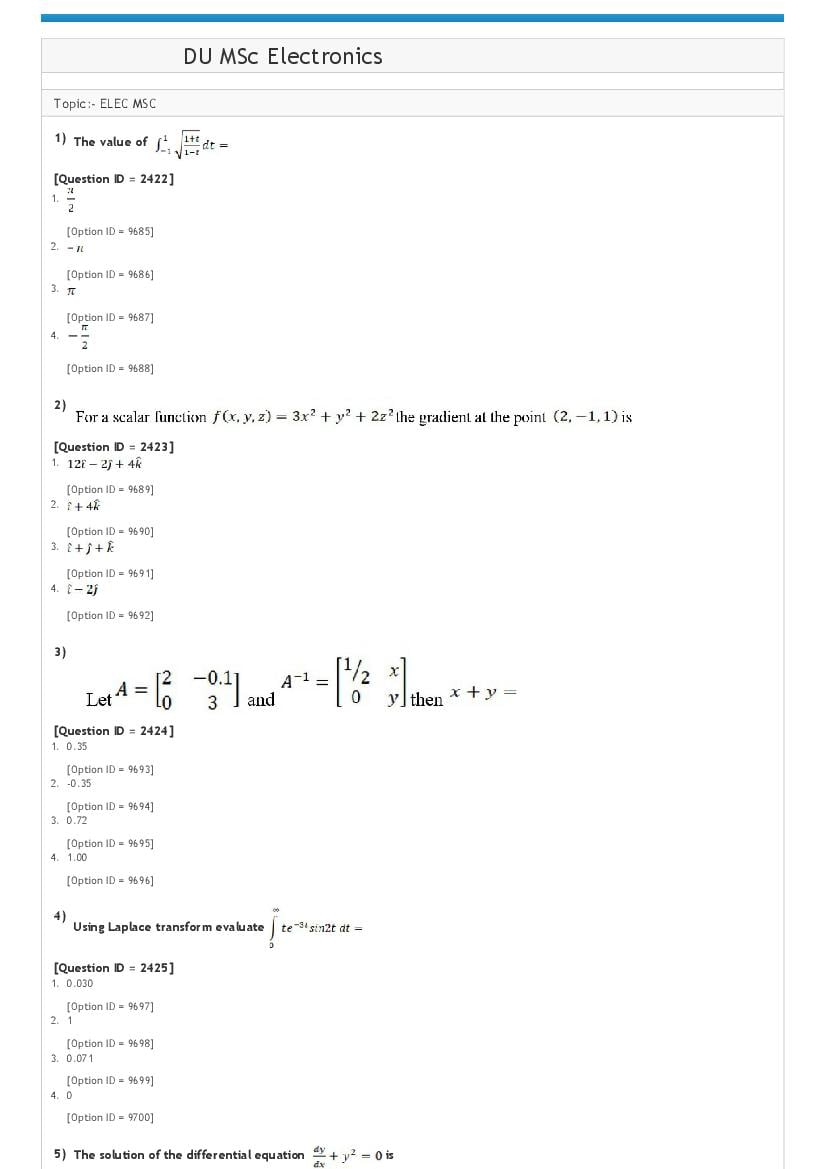
Topic:‐ ELEC MSC
1) The value of
[Question ID = 2422]
1.
[Option ID = 9685]
2.
[Option ID = 9686]
3.
[Option ID = 9687]
4.
[Option ID = 9688]
2)
[Question ID = 2423]
1.
[Option ID = 9689]
2.
[Option ID = 9690]
3.
[Option ID = 9691]
4.
[Option ID = 9692]
3)
[Question ID = 2424]
1. 0.35
[Option ID = 9693]
2. ‐0.35
[Option ID = 9694]
3. 0.72
[Option ID = 9695]
4. 1.00
[Option ID = 9696]
4)
Using Laplace transform evaluate
[Question ID = 2425]
1. 0.030
[Option ID = 9697]
2. 1
[Option ID = 9698]
3. 0.071
[Option ID = 9699]
4. 0
[Option ID = 9700]
5) The solution of the differential equation is
Page 2
1.
[Option ID = 9701]
2.
[Option ID = 9702]
3.
[Option ID = 9703]
4.
[Option ID = 9704]
6) The power internally generated within a LED, if it has internal quantum efficiency of 64.5 % and drive current of 40 mA
with a peak emission wavelength of 0.82 µm, is
[Question ID = 2427]
1. 0.09
[Option ID = 9705]
2. 0.04
[Option ID = 9706]
3. 0.06
[Option ID = 9707]
4. 0.039
[Option ID = 9708]
7) The numerical aperture of a fibre if the angle of acceptance is 45 degrees, is
[Question ID = 2428]
1. 0.50
[Option ID = 9709]
2. 0.17
[Option ID = 9710]
3. 0.75
[Option ID = 9711]
4. 0.707
[Option ID = 9712]
8) What will be the output of the following C code?
#include <stdio.h>
int main()
{
int i = 7;
i = i / 2;
printf("%d\n", i);
return 0;
}
[Question ID = 2429]
1. 2
[Option ID = 9713]
2. Error
[Option ID = 9714]
3. 3
[Option ID = 9715]
4. 1
[Option ID = 9716]
9) In C language, what is the output of the following code?
#include <stdio.h>
int main()
Page 3
printf("%d ", 1);
goto l1;
printf("%d ", 2);
l1:goto l2;
printf("%d ", 3);
l2:printf("%d ", 4);
}
[Question ID = 2430]
1. 1 4
[Option ID = 9717]
2. Compilation error
[Option ID = 9718]
3. 1 2 4
[Option ID = 9719]
4. 1 3 4
[Option ID = 9720]
10) In C language, what is the output of the following code?
#include<stdio.h>
int main()
{
int p = 10, q = 20, r;
if (r = p = 5 || q > 20)
printf("%d", r);
else
printf("No Output\n");
}
[Question ID = 2431]
1. 10
[Option ID = 9721]
2. 20
[Option ID = 9722]
3. 1
[Option ID = 9723]
4. No Output
[Option ID = 9724]
11) An electron in conduction band
[Question ID = 2432]
1. has no charge
[Option ID = 9725]
2. is bound to its parent atom
[Option ID = 9726]
3. has higher energy than an electron in the valance band
[Option ID = 9727]
4. is located near the top of the crystal
[Option ID = 9728]
12)
[Question ID = 2433]
1. 1.55 kA/cm2
Page 4
2. 7.04 kA/cm2
[Option ID = 9730]
3. 14.0 kA/cm2
[Option ID = 9731]
4. 3.52 kA/cm2
[Option ID = 9732]
13) If a BJT transistor has DC current gain
= 49 and emitter injection efficiency is 0.995 then its base transport factor = ________________
[Question ID = 2434]
1. 0.999
[Option ID = 9733]
2. 1
[Option ID = 9734]
3. 0.985
[Option ID = 9735]
4. 0.492
[Option ID = 9736]
14) The transconductance ( ) of a JFET is equal to
[Question ID = 2435]
1.
[Option ID = 9737]
2.
[Option ID = 9738]
3.
[Option ID = 9739]
4.
[Option ID = 9740]
15) If certain direct band gap semiconductor has bandgap 1.98 eV then color of emitting light by that semiconductor is
_________________
[Question ID = 2436]
1. Blue
[Option ID = 9741]
2. Red
[Option ID = 9742]
3. Yellow
[Option ID = 9743]
4. Green
[Option ID = 9744]
16) A digital meter has a 3½‐digit display and an accuracy of ± (0.6+1). The measurement accuracy for a 20 volt dc
voltage will be
[Question ID = 2437]
1. ± 11.1 %
[Option ID = 9745]
2. ± 1.1 %
[Option ID = 9746]
3. ± 2.2%
[Option ID = 9747]
4. ± 22.2%
[Option ID = 9748]
17) A permanent magnet movement coil instrument with 500 μA FSD and a 1 kΩ coil resistance is to use in an Ammeter.
The shunt resistance for a FSD of 100 mA is
Page 5
1. 10.02 W
[Option ID = 9749]
2. 50.02 W
[Option ID = 9750]
3. 1.025 W
[Option ID = 9751]
4. 5.025 W
[Option ID = 9752]
18) A basic Q‐meter circuit has 100 mV ac supply, R= 10 Ω and XL=XC=100 Ω at resonance. The Q factor of the coil is
[Question ID = 2439]
1. 10
[Option ID = 9753]
2. 50
[Option ID = 9754]
3. 40
[Option ID = 9755]
4. 20
[Option ID = 9756]
19) An 820 Ω resistance with ±10% accuracy carries a 10 mA current. The current was measured on the 25 mA range
analog meter that has ±2% accuracy of full scale. The % error in 10 mA current is
[Question ID = 2440]
1. ± 5 %
[Option ID = 9757]
2. ± 10 %
[Option ID = 9758]
3. ± 15 %
[Option ID = 9759]
4. ± 20 %
[Option ID = 9760]
20) A pulse waveform with a 10 ns rise time is applied to an oscilloscope that has an upper cutoff frequency of 10 MHz,
the displayed rise time will be
[Question ID = 2441]
1. 36.4 ns
[Option ID = 9761]
2. 25.7 ns
[Option ID = 9762]
3. 51.5 ns
[Option ID = 9763]
4. 47.6 ns
[Option ID = 9764]
21) The resonant frequency of the series circuit shown in figure is:
[Question ID = 2442]
1. 1/6π
[Option ID = 9765]
2. 1/4π
[Option ID = 9766]
3. 1/π
[Option ID = 9767]
4. 1/3π
[Option ID = 9768]
Page 6
respectively.
[Question ID = 2443]
1. 9, 3 and 1.5
[Option ID = 9769]
2. 3, 9 and 1.5
[Option ID = 9770]
3. 1.5, 3 and 9
[Option ID = 9771]
4. 3, 1.5 and 9
[Option ID = 9772]
23) A series R–L–C circuit has a Q of 100 and an impedance of (100 + j0)Ω at its resonant angular frequency of 107 rad/sec.
The values of R and L is:
[Question ID = 2444]
1. 10 Ω, 102 H
[Option ID = 9773]
2. 1000 Ω, 10 H
[Option ID = 9774]
3. 100 Ω, 100 H
[Option ID = 9775]
4. 100 Ω, 10‐3 H
[Option ID = 9776]
24) In the figure shown, the value of the current I (in Amperes) is
[Question ID = 2445]
1. 0.5
[Option ID = 9777]
2. 2
[Option ID = 9778]
3. 0
[Option ID = 9779]
4. 2.5
[Option ID = 9780]
25) A current is flowing through a conductor with non‐uniform area of cross‐section. Then
[Question ID = 2446]
1. current will be different at different cross‐sections
[Option ID = 9781]
2. current will be the same but current density will be different at different cross‐sections
[Option ID = 9782]
3. current will be the same at all the cross‐sections
[Option ID = 9783]
4. current will be different but current density will be same at all the cross‐sections
[Option ID = 9784]
26) For an RC coupled common source junction field effect transitory (JFET) amplifier without bypass capacitor, gm = 1 mΩ‐
1, source resistance is 2 kΩ, drain resistance is 15 kΩ and load is 10 kΩ. The value of voltage gain is
[Question ID = 2447]
Page 7
[Option ID = 9785]
2. 5
[Option ID = 9786]
3. ‐2
[Option ID = 9787]
4. ‐5
[Option ID = 9788]
27) A 35 mV signal is applied to the base of a properly biased transistor with re = 8 Ω and Rc = 1 kΩ. The output signal
voltage at the collector is
[Question ID = 2448]
1. 3.25 V
[Option ID = 9789]
2. 4.38 V
[Option ID = 9790]
3. 28.62 V
[Option ID = 9791]
4. 13.79 V
[Option ID = 9792]
28) For step graded diode of area 5 cm2, capacitance per unit area when no reverse bias is applied is 2 pF/cm2. What is
the net capacitance when applied reverse bias voltage is 99 V?
[Question ID = 2449]
1. 2 pF
[Option ID = 9793]
2. 0.1 pF
[Option ID = 9794]
3. 1 pF
[Option ID = 9795]
4. 5 pF
[Option ID = 9796]
29) If α = 0.995, IE = 10 mA, ICO = 0.5 μA, then ICEO will be[Question ID = 2450]
1. 25 μA [Option ID = 9797]
2. 10.1 μA [Option ID = 9798]
3. 100 μA [Option ID = 9799]
4. 10.5 μA [Option ID = 9800]
30) In a Schmitt trigger, type of feedback is[Question ID = 2451]
1. degenerative feedback [Option ID = 9801]
2. regenerative feedback [Option ID = 9802]
3. either regenerative or degenerative [Option ID = 9803]
4. neither regenerative nor degenerative [Option ID = 9804]
31) Match List I with List II
List I List II
A. I. A≠B
B. II. A=B
C. III. A=1 or B=1
D. IV. A=1 or B=0
Choose the correct answer from the options given below:
[Question ID = 2452]
1. A ‐ III, B ‐ II, C ‐ I, D ‐ IV
[Option ID = 9805]
2. A ‐ II, B ‐ III, C ‐ IV, D ‐ I
[Option ID = 9806]
3. A ‐ III, B ‐ II, C ‐ IV, D ‐ I
[Option ID = 9807]
4. A ‐ II, B ‐ III, C ‐ I, D ‐ IV
[Option ID = 9808]
32) Consider the following statements:
Page 8
B. A NOR gate is equivalent to an AND gate with its inputs inverted.
C. A NAND gate is equivalent to an OR gate with its output inverted.
D. A NOR gate is equivalent to an AND gate with its output inverted.
Choose the correct answer from the options given below:
[Question ID = 2453]
1. A and B only
[Option ID = 9809]
2. B and C only
[Option ID = 9810]
3. C and D only
[Option ID = 9811]
4. A and D only
[Option ID = 9812]
33) If XY=0 then X Y is equal to
[Question ID = 2454]
1.
[Option ID = 9813]
2. XY
[Option ID = 9814]
3.
[Option ID = 9815]
4. X+Y
[Option ID = 9816]
34) In the following circuit the output Z is
[Question ID = 2455]
1.
[Option ID = 9817]
2.
[Option ID = 9818]
3.
[Option ID = 9819]
4.
[Option ID = 9820]
35) The hexadecimal number 13AF to their decimal equivalent is:[Question ID = 2456]
1. 5039 [Option ID = 9821]
2. 5029 [Option ID = 9822]
3. 5019 [Option ID = 9823]
4. 5099 [Option ID = 9824]
36) The logic operation that will selectively clear bits in register A in those positions where there are 1’s in the bits of
register B is given by[Question ID = 2457]
1.
[Option ID = 9825]
2.
[Option ID = 9826]
3.
[Option ID = 9827]
4.
[Option ID = 9828]
37) Consider the following program intended to transfer a block of 5 bytes from A000H to 9000H
Page 9
LXI H, A000H
MVI C, 05H
LOOP: MOV A, M
STAX B
INX B
INX H
DCR C
JNZ LOOP
HLT
The above program will not work because
[Question ID = 2458]
1. C register is used as counter
[Option ID = 9829]
2. DCR C instruction will not affect zero flag
[Option ID = 9830]
3. JNZ instruction is used instead of JZ
[Option ID = 9831]
4. The first two instructions in loop should have been LDAX D and MOV M, A
[Option ID = 9832]
38) Given below are two statements
Statement I : On executing the HLT instruction, the microprocessor enters into halt state and all the buses are tri‐stated
Statement II : On executing the HLT instruction, the microprocessor is disconnected from the system bus till the reset is pressed
In light of the above statements, choose the correct answer from the options given below
[Question ID = 2459]
1. Both Statement (I) and Statement (II) are individually true but Statement (II) is not the correct explanation of Statement (I)
[Option ID = 9833]
2. Both Statement (I) and Statement (II) are individually true and Statement (II) is the correct explanation of Statement (I)
[Option ID = 9834]
3. Statement (I) is true but Statement (II) is false
[Option ID = 9835]
4. Statement (I) is false but Statement (II) is true
[Option ID = 9836]
39) Which one of the following interrupts is both level and edge sensitive?[Question ID = 2460]
1. RST 7.5 [Option ID = 9837]
2. TRAP [Option ID = 9838]
3. RST 5.5 [Option ID = 9839]
4. INTR [Option ID = 9840]
40) Consider the following statements regarding RESET instruction of 8085 microprocessor
A. PC content becomes 0000H
B. All interrupts are enabled
C. RESET OUT pin is at logic 0
Choose the correct answer from the options given below:
[Question ID = 2461]
1. B only
[Option ID = 9841]
2. A and B only
[Option ID = 9842]
3. B and C only
[Option ID = 9843]
4. A only
[Option ID = 9844]
Page 10
[Question ID = 2462]
1. 0.22 A/m
[Option ID = 9845]
2. 0.75 A/m
[Option ID = 9846]
3. 2.04 A/m
[Option ID = 9847]
4. 0.15 A/m
[Option ID = 9848]
42) In the following figure, the field E1 makes an angle of q1 with the axis normal to the boundary line, while the field E2
makes an angle of q2 in medium 2. The ratio of normal components of E2 over E1 (i.e. En2/En1) is
[Question ID = 2463]
1. 2 [Option ID = 9849]
2. 1/2 [Option ID = 9850]
3. 4 [Option ID = 9851]
4. 1/4 [Option ID = 9852]
43) If the flux density in a certain magnetic material is 0.25 T and the area of the material is 25 mm2. The magnetic flux
through material is
[Question ID = 2464]
1. 2.5 μWb
[Option ID = 9853]
2. 0.5 μWb
[Option ID = 9854]
3. 6.25 μWb
[Option ID = 9855]
4. 25 μWb
[Option ID = 9856]
44) A parallel‐plate capacitor is formed with a mica dielectric er = 6, a plate area of 10 mm2 and a separation of 0.01 mm2.
If the potential difference between the lower and upper plates is 100V, the total charge stored in capacitor
is
[Question ID = 2465]
1. 12.00 μC
[Option ID = 9857]
2. 5.31 μC
[Option ID = 9858]
3. 62.46 μC
[Option ID = 9859]
4. 10.78 μC
[Option ID = 9860]
45)
[Question ID = 2466]
1.
[Option ID = 9861]
2.
[Option ID = 9862]
3.
[Option ID = 9863]
4.
Page 11
46) A 10MHz carrier is frequency modulated by a sinusoidal signal of 500 Hz, the maximum frequency deviation being 50
kHz. The bandwidth required, as given by Carson’s rule is[Question ID = 2467]
1. 100 kHz [Option ID = 9865]
2. 99 kHz [Option ID = 9866]
3. 101 kHz [Option ID = 9867]
4. 98 kHz [Option ID = 9868]
47) In a PCM system with uniform quantization, increasing the number of bits from 8 to 9 will reduce the quantization noise
power by a factor of
[Question ID = 2468]
1. 2
[Option ID = 9869]
2. 9
[Option ID = 9870]
3. 8
[Option ID = 9871]
4. 4
[Option ID = 9872]
48) A device with input x(t) and output y(t) is characterized by: y(t) = x2(t). An FM signal with frequency deviation of 90
kHz and modulating signal bandwidth of 5 kHz is applied to this device. The bandwidth of the output signal is
[Question ID = 2469]
1. 190 kHz
[Option ID = 9873]
2. 370 kHz
[Option ID = 9874]
3. 380 kHz
[Option ID = 9875]
4. 95 kHz
[Option ID = 9876]
49) An analog baseband signal, bandlimited to 100 Hz, is sampled at the Nyquist rate. The samples are quantized into four
message symbols that occur independently with probabilities p1 = p4 = 0.125 and p2 = p3. The information rate (bits/sec) of
the message source is
[Question ID = 2470]
1. 2.813 bits/sec
[Option ID = 9877]
2. 1.11 bits/sec
[Option ID = 9878]
3. 0.125 bits/sec
[Option ID = 9879]
4. 1.811 bits/sec
[Option ID = 9880]
50)
[Question ID = 2471]
1. 20%
[Option ID = 9881]
2. 11.11%
[Option ID = 9882]
3. 8.33%
[Option ID = 9883]
4. 25%
[Option ID = 9884]
Document Details
| Board / Org | NTA |
| Exam | DUET |
| Type | Question Paper |
| Pages | 11 |
| Language | english |
| Updated | 30 Apr 2026 |