Goa Board Class 12 Question Paper 2025 Electronic Material & Workshop Practice
Finished viewing? Save it for later —
Download Goa Board Class 12 Question Paper 2025 Electronic Material & Workshop Practice (PDF · 4 pages)About Goa Board Class 12 Question Paper 2025 Electronic Material & Workshop Practice
Goa Board Class 12 Question Paper 2025 Electronic Material & Workshop Practice is available here for free download. Published by Goa Board for Class 12, this question paper can be viewed online or downloaded as a PDF (4 pages). Candidates preparing for Class 12 can use Goa Board Class 12 Question Paper 2025 Electronic Material & Workshop Practice to understand the exam pattern, the type of questions asked, and the overall difficulty level.
Frequently Asked Questions
How can I download Goa Board Class 12 Question Paper 2025 Electronic Material & Workshop Practice?
Open this page and click the Download button to save Goa Board Class 12 Question Paper 2025 Electronic Material & Workshop Practice as a PDF. It is completely free on AglaSem Docs.
Is Goa Board Class 12 Question Paper 2025 Electronic Material & Workshop Practice free to download?
Yes. Goa Board Class 12 Question Paper 2025 Electronic Material & Workshop Practice can be viewed online and downloaded as a PDF free of cost on AglaSem Docs.
How many pages does Goa Board Class 12 Question Paper 2025 Electronic Material & Workshop Practice have?
Goa Board Class 12 Question Paper 2025 Electronic Material & Workshop Practice contains 4 pages, which you can read online or download together as a single PDF.
Where can I find more Class 12 study material?
You can find more Class 12 question papers, sample papers, syllabus, and answer keys on AglaSem Docs.
Goa Board Class 12 Question Paper 2025 Electronic Material & Workshop Practice – Text
Read the full text of this question paper below — useful to quickly search, copy and reference the content online without downloading the PDF.
📄 View text version (4 pages)
Page 1
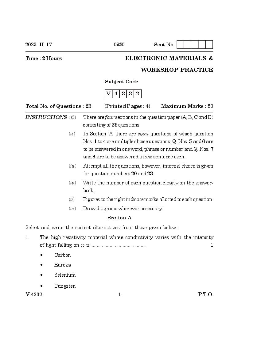
Time : 2 Hours ELECTRONIC MATERIALS &
WORKSHOP PRACTICE
Subject Code
V 4 3 3 2
Total No. of Questions : 23 (Printed Pages : 4) Maximum Marks : 50
INSTRUCTIONS : (i) There are four sections in the question paper (A, B, C and D)
consisting of 23 questions.
(ii) In Section ‘A’ there are eight questions of which question
Nos. 1 to 4 are multiple choice questions, Q. Nos. 5 and 6 are
to be answered in one word, phrase or number and Q. Nos. 7
and 8 are to be answered in one sentence each.
(iii) Attempt all the questions, however, internal choice is given
for question numbers 20 and 23.
(iv) Write the number of each question clearly on the answer-
book.
(v) Figures to the right indicate marks allotted to each question.
(vi) Draw diagrams wherever necessary.
Section A
Select and write the correct alternatives from those given below :
1. The high resistivity material whose conductivity varies with the intensity
of light falling on it is .......................................... 1
• Carbon
• Eureka
• Selenium
• Tungsten
V-4332 1 P.T.O.
Page 2
• Bimetallic relay
• Dry reed relay
• General purpose relay
• Mercury wetted relay
3. The insulating material obtained by combination of Acetylene and Hydrogen
chloride in presence of catalyst at 50ºC is ..................................... 1
• Mica
• Porcelain
• Polyvinyl chloride
• Varnish
4. Band gap of Silicon material is ................................. 1
• 0.3 eV
• 0.7 eV
• 1.21 eV
• 2.6 eV
5. Name the device used for measuring higher temperature above 357ºC at
remote places. 1
6. State the percentage composition of Eureka. 1
7. Define Insulation resistance. 1
8. Draw a neat labelled energy level diagram for semiconductor. 1
Section B
9. What is Mass soldering technique ? Name any two methods of mass
soldering. 2
V-4332 2
Page 3
(Mention two points). 2
11. Draw neat labelled diagrams for the following : 2
(a) Open circuit fault by series test lamp
(b) Resistance measurement using Voltmeter Ammeter method.
12. State any four advantages of PCB. 2
13. What is lubrication ? State any two methods of lubrication. 2
14. What is short circuit fault ? State any two causes of short circuit. 2
Section C
15. Write any four properties and two applications of Silicon steel. 3
16. State any two applications of the following Insulating materials : 3
(a) Mica
(b) Porcelain
(c) Varnish.
17. State any four properties and two applications of Germanium. 3
18. State any one application of each of the following tools : 3
(a) Adjustable wrench
(b) Bench vice
(c) Claw hammer
(d) Long nose plier
(e) Test lamp
(f) Triangular file.
V-4332 3 P.T.O.
Page 4
20. State any six points of upkeeping arrangements to be taken while working
in an Assembly Workshop. 3
Or
Write any six points of personal safety precautions to be taken in an
Assembly Workshop.
Section D
21. With a neat labelled diagram, explain Zone refining method of semiconductor
crystal growth. 4
22. State any two applications of the following Conducting materials : 4
(a) Aluminium
(b) Carbon
(c) Eureka
(d) Tungsten.
23. With the help of a neat labelled diagram, explain the construction of
Bimetallic relay. 4
Or
With the help of a neat labelled diagram, explain the construction of General
purpose relay.
V-4332 4
Document Details
| Board / Org | Goa Board |
| Exam | Class 12 |
| Type | Question Paper |
| Pages | 4 |
| Updated | 24 Sep 2026 |