MAHA SET 2025 Paper II Electronic Science Set A Question Paper
Finished viewing? Save it for later —
Download MAHA SET 2025 Paper II Electronic Science Set A Question Paper (PDF · 28 pages)About MAHA SET 2025 Paper II Electronic Science Set A Question Paper
MAHA SET 2025 Paper II Electronic Science Set A Question Paper is available here for free download. Published by Maharashtra Exams for MAHA SET, this question paper can be viewed online or downloaded as a PDF (28 pages). Candidates preparing for MAHA SET can use MAHA SET 2025 Paper II Electronic Science Set A Question Paper to understand the exam pattern, the type of questions asked, and the overall difficulty level.
Frequently Asked Questions
How can I download MAHA SET 2025 Paper II Electronic Science Set A Question Paper?
Open this page and click the Download button to save MAHA SET 2025 Paper II Electronic Science Set A Question Paper as a PDF. It is completely free on AglaSem Docs.
Is MAHA SET 2025 Paper II Electronic Science Set A Question Paper free to download?
Yes. MAHA SET 2025 Paper II Electronic Science Set A Question Paper can be viewed online and downloaded as a PDF free of cost on AglaSem Docs.
How many pages does MAHA SET 2025 Paper II Electronic Science Set A Question Paper have?
MAHA SET 2025 Paper II Electronic Science Set A Question Paper contains 28 pages, which you can read online or download together as a single PDF.
Where can I find more MAHA SET study material?
You can find more MAHA SET question papers, sample papers, syllabus, and answer keys on AglaSem Docs.
MAHA SET 2025 Paper II Electronic Science Set A Question Paper – Text
Read the full text of this question paper below — useful to quickly search, copy and reference the content online without downloading the PDF.
📄 View text version (29 pages)
Page 1
MAHA SET 2025
Paper II Electronic
Science Set A
Question Paper
EXAM YEAR TYPE
MAHA SET 2025 Question Paper
Notes · Sample Papers · Previous Year Papers · Mock Tests
Page 2
m .co s e m
l a
ag
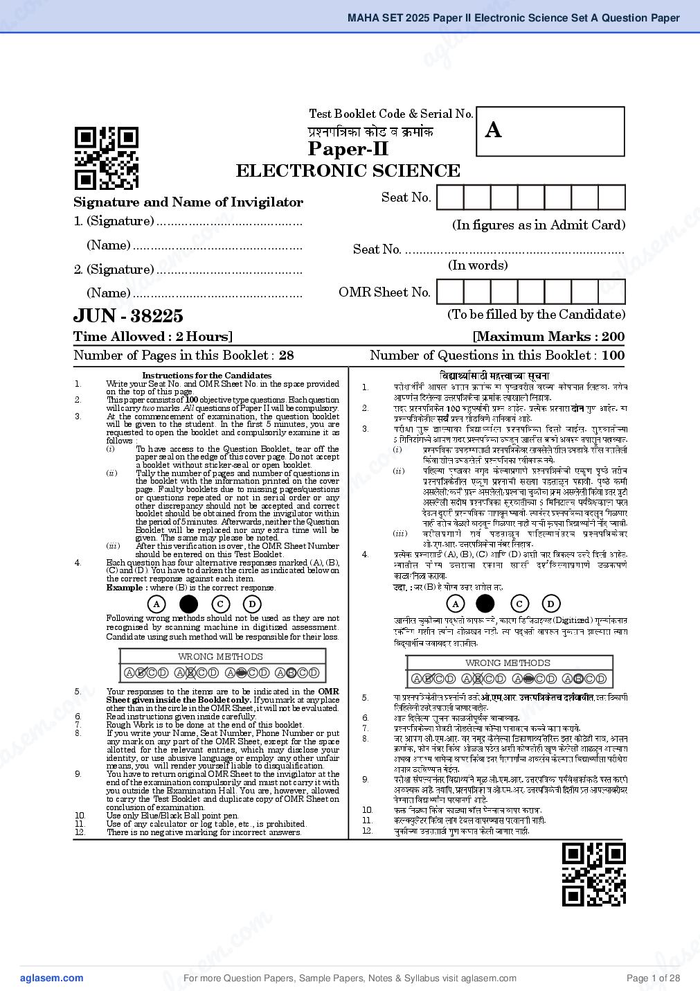
Test Booklet Code & Serial No.
A
Paper-II
ELECTRONIC SCIENCE
Signature and Name of Invigilator Seat No.
m
1. (Signature) .........................................
. co
c. o
(In figures as in Admit Card)
e m
(Name) ................................................
em
Seat No. ..............................................................
l as
s
2. (Signature) .........................................
la
(In words)
ag
g
(Name) ................................................
JUNa- 38225
OMR Sheet No.
(To be filled by the Candidate)
Time Allowed : 2 Hours] [Maximum Marks : 200
Number of Pages in this Booklet : 28 Number of Questions in this Booklet : 100
Instructions for the Candidates
1. Write your Seat No. and OMR Sheet No. in the space provided 1.
on the top of this page.
2. This paper consists of 100 objective type questions. Each question
will carry two marks. All questions of Paper II will be compulsory. 2.
3. At the commencement of examination, the question booklet
will be given to the student. In the first 5 minutes, you are
requested to open the booklet and compulsorily examine it as 3.
m
follows :
c. o
(i) To have access to the Question Booklet, tear off the (i)
paper seal on the edge of this cover page. Do not accept
a booklet without sticker-seal or open booklet.
(ii)
m
(ii) Tally the number of pages and number of questions in
e
the booklet with the information printed on the cover
s
page. Faulty booklets due to missing pages/questions
a
or questions repeated or not in serial order or any
l
other discrepancy should not be accepted and correct
ag
booklet should be obtained from the invigilator within
the period of 5 minutes. Afterwards, neither the Question
Booklet will be replaced nor any extra time will be (iii)
given. The same may please be noted.
(iii) After this verification is over, the OMR Sheet Number
should be entered on this Test Booklet. 4. (A), (B), (C) (D)
4. Each question has four alternative responses marked (A), (B),
(C) and (D). You have to darken the circle as indicated below on
the correct response against each item.
Example : where (B) is the correct response. (B)
A C D A C D
Following wrong methods should not be used as they are not (Digitized)
recognised by scanning machine in digitized assessment.
Candidate using such method will be responsible for their loss.
CORRECT METHOD WRONG METHODS
CORRECT METHOD WRONG METHODS
C D A B C D A B C D A B C D A B C D
m
c. o
C D A B C D A B C D A B C D A B C D
m
5. Your responses to the items are to be indicated in the OMR
.co
5.
m
Sheet given inside the Booklet only. If you mark at any place
e
other than in the circle in the OMR Sheet, it will not be evaluated.
s
6. Read instructions given inside carefully. 6.
e m 7.
8.
Rough Work is to be done at the end of this booklet.
If you write your Name, Seat Number, Phone Number or put
7.
la
s g
any mark on any part of the OMR Sheet, except for the space 8.
la a
allotted for the relevant entries, which may disclose your
identity, or use abusive language or employ any other unfair
means, you will render yourself liable to disqualification.
9. You have to return original OMR Sheet to the invigilator at the
end of the examination compulsorily and must not carry it with 9.
you outside the Examination Hall. You are, however, allowed
to carry the Test Booklet and duplicate copy of OMR Sheet on
conclusion of examination. 10.
10. Use only Blue/Black Ball point pen.
11. Use of any calculator or log table, etc., is prohibited. 11.
12. There is no negative marking for incorrect answers. 12.
m
.co s e
s em
For more Question Papers, Sample Papers, Notes & Syllabus visit
gl a
Page 1 of 28
Page 3
For more Question Papers, Sample Papers, Notes & Syllabus visit Page 2 of 28
Page 4
m .co s e m
l a
ag
Electronic Science
Paper II
co
Time Allowed : 120 Minutes] [Maximum Marks : 200
. c om
Note : This Paper contains Hundred (100) multiple choice questions. Each question
carrying Two (2) marks. Attempt All questions.
e m .
e m as
s 2. In semiconductor manufacturing, l
1.
g l a
In the semiconductors, what is the ag?
a what does the term wafer refer to
role of a doping ? (A) A thin slice of single-crystal
semiconductor material
(A) It increases the bandgap of the (B) The metallic layer on top of a
semiconductor device
semiconductor material (C) The insulation material
o m between different
(B) It introduces impurities to
m .c semiconductor layers
s e
l a (D) The encapsulation material
ag
modify the electrical properties
used in semiconductor
packaging
of the material
3. In a Zener diode, what is the
primary role of the depletion
(C) It enhances the thermal
region ?
(A) To increase the forward bias
conductivity of the
current
m
m (B) To provide mechanical support
.co
.co em
semiconductor
e m s
to the diode
la the reverse
las (D) It decreases the resistivity of g
(C) To enhance
a voltage
breakdown
(D) To reduce the capacitance of the
the semoconductor material
diode
3 [P.T.O.
m
.co s e
s em
For more Question Papers, Sample Papers, Notes & Syllabus visit
gl a
Page 3 of 28
Page 5
does the open-circuit voltage ( Voc )
passage of light to create different
represent ?
colors ?
(A) The maximum voltage the cell
(A) By changing the pixel’s size can generate under
(B) By altering the liquid crystal illumination
alignment (B) The voltage when the cell is not
exposed to light
(C) By adjusting the backlight
(C) The voltage when the current
intensity
is zero
(D) By using a color filter
(D) The voltage when the cell is at
5. What is the primary role of barrier maximum power point
layers in quantum well devices ? 7. What is the significance of the
‘‘quantum Hall effect’’ observed in
(A) To increase carrier
graphene ?
concentration (A) It indicates the presence of a
bandgap in graphene
(B) To enhance thermal
(B) It demonstrates the unique
conductivity
behavior of charge carriers in
(C) To confine charge carriers in graphene
one dimension (C) It signifies the low thermal
conductivity of graphene
(D) To reduce the overall device
(D) It is unrelated to the electronic
size
properties of graphene
4
For more Question Papers, Sample Papers, Notes & Syllabus visit Page 4 of 28
Page 6
m .co s e m
l a
ag
8. What is the unique structural 10. What is the primary advantage of
feature of a carbon nanotube that
om
LED technology over traditional
. co
. c e m
e m
contributes to its exceptional
incandescent lighting ?
l as
l as
strength ? ag
ag (A) Higher power consumption
(A) Planar hexagonal lattice
(B) Longer lifespan
(B) Rolling vector
(C) Limited color options
(C) Quasi-one-dimensional structure
(D) Lower efficiency
m
.co
(D) Hexagonal Closed Packed
Structure
e m11. In X-ray Diffractometers, line
l as
ag
9. What are potential applications of intensities depend on .............. and
ZnO in the field of optoelectronics ? kind of atomic reflection centres in
(A) Photovoltaic cells and light- each set of plates.
emitting diodes (LEDs)
(A) Number
m
.co
(B) Quantum computing devices
m
.co
(B) Position
e m
e m
(C) Superconductors and magnetic
as
s (C) Length gl
la storage
a
(D) Gas sensors and fuel cells (D) Distance between lines
5 [P.T.O.
m
.co s e
s em
For more Question Papers, Sample Papers, Notes & Syllabus visit
gl a
Page 5 of 28
Page 7
Diffractogram represents :
MOS system when gate voltage is
(A) Amorphous Material zero is :
(B) Polymeric Material
Ec
(C) Highly Crystalline Structure Ei
(A) E Fm EFp
Ev
Metal (A) Semiconductor (S)
Oxide
(D) Conductor Material p-type
13. The chemical used for shielding the Metal (A) Oxide Semiconductor (S)
p-type
active areas to achieve selective
Ec
oxide growth is : Ei
(B) EFp
qVo Ev
(A) Silver Nitride E Fm
(B) Silicon Nitride
Metal (A) Oxide Semiconductor (S)
(C) Hydrofluoric acid p-type
EFm
Ec
(D) Polysilicon qVo
(C) Ei
EFp
Ev
14. The scaling factor of current density
in constant voltage model is :
Metal (A) Oxide
(A) 1/2
Semiconductor (S)
p-type
(B) 1 Ec
(D) Ei
qVo EFp
(C) 2 E Fm Ev
(D) 2 /
6
For more Question Papers, Sample Papers, Notes & Syllabus visit Page 6 of 28
Page 8
m .co s e m
l a
ag
16. What is the Primary Function of the 19. Which of the following is used to
Shift Register in A CCD ?
om
obtain silicon single crystal structure
. co
. c e m
em
(A) Data storage while fabricating integrating
l as
(B) l as ag
ag Serial transfer of charge circuits ?
(C) Analog-to-digital conversion
(A) Oxidation
(D) Image processing
(B) Epitaxial growth
17. Which of the following design styles
(C) Photolithography
provides higher integration density ?
m
c. o(D) Silicon wafer preparations
(A) Switch transistor logic
e m
l as
(B) Transistor buffer logic g
a 20. The pull up to pull down impedance
(C) Transistor transistor logic ratio for an nMOS inverter driven
(D) Circuit level logic by another nMOS inverter is .........
18. Which gives scalable design rules ?
(A) 8/1
m
m (A) Lambda rules
.co
.co m
(B) 4/1
m s e
e la
(B) Micron rules
las (C) 8/3
ag
(C) Layer rules
(D) 1/4
(D) Thickness rules
7 [P.T.O.
m
.co s e
s em
For more Question Papers, Sample Papers, Notes & Syllabus visit
gl a
Page 7 of 28
Page 9
theorem ? to in network analysis ?
(A) Simplify parallel circuits (A) A set of parallel resistors
(B) Analyse AC circuits (B) A set of series resistors
(C) Calculate equivalent resistance (C) A combination of resistors and
capacitors
(D) Determine open-circuit voltage
(D) A set of branches that, if cut,
22. Norton’s equivalent current is in
will divide the network into two
parallel with :
parts
(A) A resistor
25. In filter design, what is the purpose
(B) A capacitor
of the Butterworth approximation ?
(C) An inductor
(A) To achieve a maximally flat
(D) A voltage source response in the passband
23. The Laplace transform of a unit (B) To minimize phase distortion in
impulse function is : the stopband
(A) 1/s (C) To maximize the bandwidth of
(B) e–st the filter
(C) (t) (D) To ensure equal ripple in both
the passband and stopband
(D) 1
8
For more Question Papers, Sample Papers, Notes & Syllabus visit Page 8 of 28
Page 10
m .co s e m
l a
ag
26. What does the term ‘‘poles and zeros
28. In filter design, what is the
co
cancellation’’ imply in control system
theory ?
. c om significance of the transition
e m .
e m l as
l as
(A) It results in an unstable system bandwidth ?
ag
g
a It improves the transient
(B) (A) It represents the range of
response of the system
frequencies with equal ripple in
(C) It simplifies the transfer
the stopband
function of the system
(D) It reduces the order of the
m(B) It indicates the sharpness of the
c. o
system
e m
l as frequency transition between
a g
27. What is the purpose of the Routh-
passband and stopband
Hurwitz stability criterion ?
(A) To determine the stability of a (C) It is the range of frequencies
control system
over which the filter exhibits a
(B) To analyse power distribution
maximally flat response
m
.co
in electrical grids
m
m .co (C) To optimize the bandwidth of a
s em
(D) It defines the frequency range
s e in whichg
la
la a
communication system the filter has minimal
(D) To design filters with optimal
group delay
frequency response
9 [P.T.O.
m
.co s e
s em
For more Question Papers, Sample Papers, Notes & Syllabus visit
gl a
Page 9 of 28
Page 11
significance of the transition
represent in the context of a JFET ?
bandwidth ?
(A) It represents the range of (A) Drain current
frequencies with equal ripple in
(B) Gate-source voltage
the stopband
(B) It indicates the sharpness of the (C) Gate current when the gate-
frequency transition between
source junction is forward-
passband and stop-band
biased
(C) It is the range of frequencies
over which the filter exhibits a (D) Gate current when the gate-
maximally flat response
source junction is reverse-biased
(D) It defines the frequency range
in which the filter has minimal 32. What information does the
group delay measurement of dc beta provide
30. The multiplication of two discrete about a bipolar junction transistor ?
Fourier transforms (DFTs) is equal
to the ............... of two sequences in (A) Voltage drop across the collector
the time domain. resistor
(A) Circular convolution
(B) Gain bandwidth product
(B) Auto-correlation
(C) Current gain characteristics
(C) Linear convolution
(D) Cross-correlation (D) Base-emitter voltage threshold
10
For more Question Papers, Sample Papers, Notes & Syllabus visit Page 10 of 28
Page 12
m.co s e m
l a
ag
33. What is the purpose of inverting 35. Which of the following is true about
co
the FET as its advantage ?
(–) and non-inverting (+) input
. om
c an operational (A) Low input resistance
e m .
terminals
e m on
l as
l as
amplifier ? (B) High output resistance
ag
ag
(A) Determine Op-Amp’s power (C) Big size, small life
supply (D) Better thermal stability
36. What is fractional –N frequency
(B) Control gain of Op-Amp
synthesis in PLLs and is it used ?
(C) Define the amount of feedback
m
c. o(A) It involves using fractional
(D) Provide input signals for
e m
as
values in the frequency divider
differential amplificationgl to achieve finer frequency
a resolution
34. The phase difference between the
(B) It utilizes non-integer division
input and output voltages in a
ratios to improve phase noise
common base arrangement is .........
performance
(A) 180º
o m
(C) It refers to using fractional
m c
. voltage
.co (B) 90º e m
values VCO control
s
em la to eliminate
las ag
(D) It is technique
(C) 270º
spurious signals in the PLL
(D) 0º output
11 [P.T.O.
m
.co s e
s em
For more Question Papers, Sample Papers, Notes & Syllabus visit
gl a
Page 11 of 28
Page 13
suited for ..........
where high stability of frequency is
required. (A) Detection of signal from
photodiode
(A) Wien bridge
(B) Detection of output from load
(B) Crystal
cell
(C) Hartley
(C) Detection of signal from
(D) Colpitts distance stars
(D) Detection of signal from RF
38. Which of the following ICs is the
transponder
standard IC used for V to F
40. Which of the following IC does not
conversion ?
belong to voltage regulator class ?
(A) 741
(A) 7805
(B) 7400
(B) 7905
(C) 566
(C) LM 723
(D) 723
(D) NE536
12
For more Question Papers, Sample Papers, Notes & Syllabus visit Page 12 of 28
Page 14
m .co s e m
l a
ag
41. What type of gates are NAND and 44. In a 4-bit ripple counter, how many
co
NOR gates considered to be ? clock pulse are required for a
. c om complete counting cycle ?
e m .
(A) Special-purpose gates
e m l as
l as
(B) Complex gates
(A) 4
ag
ag (B) 8
(C) Standard logic gates
(C) 16
(D) Outdated gates
(D) 2
42. What is the primary building block
45. .............. is used to carry digital data
of a CPLD ?
o m analog lines.
on
(A) Flip-flop
m .c
s e (A) Modem
(B) Gate
l a
(C) Block RAM
ag (B) Demodulator
(C) Modulator
(D) Macro cell
(D) Multiplexer
43. What is the primary building block 46. Modulo 6 counter can be built with
of an FPGA ? .............. flip flops.
m
m .co
.co
(A) Macro cell (A) 2
e m
e m (B) 3
las
las (B) Gate
ag
(C) Look-Up Table (LUT) (C) 4
(D) 6
(D) Flip-flop
13 [P.T.O.
m
.co s e
s em
For more Question Papers, Sample Papers, Notes & Syllabus visit
gl a
Page 13 of 28
Page 15
have access only to leftmost and combinational circuit.
rightmost feedback : (A) Shift Registers
(A) Parallel in serial out register (B) Counters
(B) Serial in serial out register (C) Flip flops
(C) Shift left and shift right register
(D) Multiplexers
(D) Serial in parallel out register
51. Why do we need a ULN2003 in
48. In FSM diagram what does circle driving a stepper motor from 8051
represent ? port ?
(A) State (A) for switching the motor ON and
(B) Change of state OFF
(C) Output value (B) for increasing the current
(D) Initial state (C) for increasing the power
49. ................... are employed to specify (D) for auto shut off on short circuit
parameters that can be supplied to 52. Which of the following signal
VHDL entities. controls the flow of data ?
(A) Port numbers (A) RTS
(B) Packages (B) DTR
(C) Declarations (C) RTS and DTR
(D) Generics (D) ECNR
14
For more Question Papers, Sample Papers, Notes & Syllabus visit Page 14 of 28
Page 16
m .co s e m
l a
ag
53. If we push data onto the stack, then 55. The function of Execution Unit is :
co
the stack pointer :
o m every push
(A) increases cwith
(A) Encoding
m .
m . s e
s e with every push (B) Decoding
g l a
g l a
(B) decreases
a
a increases and decreases with
(C)
(C) Processing
every push (D) Calculations
(D) doesn’t change
56. The JS is called as ...............
54. What steps are followed when we
(A) jump the signed bit
need to turn on any timer ?
m
(A) load the count, start the timer, c. o(B) jump single bit
e m
keep monitoring it, stop the
l as (C) jump simple bit
timer ag (D) jump signal it
(B) load the TMOD register, load the
57. Which microprocessor accepts the
count, start the timer, keep
program written for 8086 without
monitoring it, stop the timer
any changes ?
(C) load the TMOD register, start
m
m the timer, load the count, keep (A) 8085
.co
m .co monitoring it, stop the timer
s e m
e la
(B) 8051
las g
(C) 8057 a
(D) load the count, divide TCON by
2, start the timer, keep
monitoring it, stop the timer (D) 8088
15 [P.T.O.
m
.co s e
s em
For more Question Papers, Sample Papers, Notes & Syllabus visit
gl a
Page 15 of 28
Page 17
List I have the option of using the .........
(1) TCON ROM or EPROM together with .......
(2) SBUF
memory and devices.
(3) TMOD
(A) EA, high, internal, external
(4) PSW
(B) EA, low, internal, external
(5) PCON
List II (C) EA, high, external, internal
(i) contains status information
(D) EA, low, external internal
(ii) timer/counter control register
60. Which of the following Buses is/are
(iii) idle bit, power down bit
present in a microcontroller for
(iv) serial data buffer for Tx and Rx
transferring data from one place to
(v) timer/counter modes of
operation another ?
Codes : (A) Data bus only
(1) (2) (3) (4) (5)
(B) Data Bus, Address Bus
(A) (ii) (iv) (v) (i) (iii)
(C) Address Bus
(B) (i) (v) (iv) (iii) (ii)
(C) (v) (iii) (ii) (iv) (i) (D) Address Bus, Data Bus, Control
(D) (iii) (ii) (i) (v) (iv) Bus
16
For more Question Papers, Sample Papers, Notes & Syllabus visit Page 16 of 28
Page 18
m .co s e m
l a
ag
61. In charge free space, the Poisson 64. In free space, which of the following
co
equation becomes :
om .
will be zero ?
(A) Maxwell.c
equation
e m
e m (A) Permittivity
l as
las
(B) Ampere equation
ag
g
a Laplace equation (B) Permeability
(C)
(D) Steady state equation (C) Conductivity
62. The total number of magnetic field (D) Resistivity
lines passing through an area is
termed as : m
65. A wave incident on a surface at an
c. oangle 60 degree is having field
(A) Voltage
e m
l as
ag
intensity of 6 units. The reflected
(B) EMF
wave is at an angle of 30 degrees.
(C) Magnetic flux
Find the field intensity after
(D) Magnetic flux density
reflection.
63. Which of the following laws does not
form a Maxwell equation ? (A) 9.4
m
m (A) Planck’s law .co
m .co (B) 8.4
s e m
s e (B) Gauss’s Law
(C) 10.4 ag
la
la (C) Faraday’s law
(D) 7.4
(D) Ampere’s Law
17 [P.T.O.
m
.co s e
s em
For more Question Papers, Sample Papers, Notes & Syllabus visit
gl a
Page 17 of 28
Page 19
antenna having a power of 120 units
is :
and antenna current of 5A is :
(A) Dielectric waveguide propagation
(A) 4.8
(B) Conductor propagation (B) 9.6
(C) Cavity resonator propagation (C) 3.6
(D) 1.8
(D) Not practically possible
69. Copper behaves as a :
67. An example for usage of
(A) Conductor always
electromagnetic wave propagation
(B) Conductor or dielectric
is : depending on the applied
electric field strength
(A) refrigerator
(C) Conductor or dielectric
(B) electric fan depending on the frequency
(D) Conductor or dielectric
(C) mobile transponder
depending on the electric
(D) relays in actuators current density
18
For more Question Papers, Sample Papers, Notes & Syllabus visit Page 18 of 28
Page 20
m .co s e m
l a
ag
70. The modes in a rectangular 72. The characteristic of a radio receiver
waveguide are denoted by TEmn/ associated with true reproduction of
om
TMmn, where m and n are the Eigen audio signal is : . co
. c e m
em
values along the larger and smaller
(A) Sensitivity
l as
as
dimensions of the waveguide
l ag
ag
respectively. Which one of the
(B) Selectivity
following statements is true ? (C) Image rejection
(A) The TM10 mode does not exist (D) Fidelity
(B) The TE10 mode does not exist 73. The wavelength for a frequency of
25 MHz is :
(C) The TE10 and TM10 both exist
m
and have same cut-off
c. o(A) 15 metres
frequencies
e m
l as (B) 4 metres
ag
(D) When m and n are increased, (C) 12 metres
the cut-off frequency decreases
(D) 32 metres
71. The refractive index variation of a
74. Which of the following is
singal mode fiber is :
disadvantage of FM over AM ?
(A) Gradual from core to cladding (A) less modulating power is
m
.co
(B) Increasing from core to cladding required
m
m .co (C) Step change from core to
s em
(B) better noise immunity is
e provided la
las cladding
a g
(C) higher bandwidth is required
(D) Linear change from core to
cladding (D) carrier is of any shape
19 [P.T.O.
m
.co s e
s em
For more Question Papers, Sample Papers, Notes & Syllabus visit
gl a
Page 19 of 28
Page 21
of a two stage cascade network is a large amount in multimode step
8 dB and the noise figure of the index fiber results in ................ .
second stage is 7 dB and the gain
(A) Propagation of the fiber
of the first stage is 10, then the noise
(B) Propagating through the fiber
figure of the cascade is :
(C) Pulse broadening at output
(A) 8.6 dB
(D) Attenuation of waves
(B) 7.6 dB
(C) 5.6 dB 78. The internal quantum efficiency of
LEDs decreases ..............................
(D) 8.9 dB
with temperature.
76. Bluetooth is an example of :
(A) Exponentially, decreasing
(A) Wide area network
(B) Exponentially increasing
(B) Virtual private network
(C) Linearly, increasing
(C) Local area network
(D) Linearly, decreasing
(D) Personal area network
20
For more Question Papers, Sample Papers, Notes & Syllabus visit Page 20 of 28
Page 22
m .co s e m
l a
ag
81. In a SCR circuit, the angle of
79. Which technology is used by the
co
conduction can be changed by
. c om
backscatter measurement method ?
changing :
e m .
em l as
as
(A) Refraction
l
(A) anode voltage
ag
ag (B) anode current
(B) Francis flat recovery
(C) forward current rating
(C) Optical time domain
(D) gate current
reflectometry
82. A half-wave thyristor converter
m
(D) Optical frequency c. osupplies a purely inductive load, as
e m shown in Fig. If the triggering angle
as
80. Which of the following is the lway
ag
of the SCR is 120º, the extinction
angle will be :
in which an IoT device is associated
with data ?
+
Vinsin t L
(A) Internet
m
m (A) 240º
.co
.co
(B) Cloud
e m
e m (B) 180º
las
las (C) Automata
ag
(C) 200º
(D) Network
(D) 120º
21 [P.T.O.
m
.co s e
s em
For more Question Papers, Sample Papers, Notes & Syllabus visit
gl a
Page 21 of 28
Page 23
when SCR1 is fired :
supplied from a fixed voltage dc
(A) positive peak of the ac O/P is
source feeds afixed-resistive-
obtained
inductive load and a free-wheeling
(B) negative peak of the O/P is
diode. The chopper operates at 1 kHz
obtained
and 50% duty cycle. Without
(C) two-third to peak value is
changing the value of the average
obtained
dc current through the load, if it is
(D) one-third of the peak value is
desired to reduce the ripple content obtained
of load current, the control action
85. It is required to drive a d.c. shunt
needed will : motor at different speeds in both the
directions (forward and reverse) and
(A) increase the chopper frequency
also to break it in both the directions
and duty cycle in equal ratio
which one of the following would you
(B) increase the chopper frequency use ?
keeping the duty cycle constant (A) a half-controlled thyristor-
bridge
(C) decrease only the chopper
(B) a full-controlled thyristor-bridge
frequency
(C) a dual converter
(D) decrease only the duty cycle
(D) a diode bridge
22
For more Question Papers, Sample Papers, Notes & Syllabus visit Page 22 of 28
Page 24
m .co s e m
l a
ag
86. The speed and torque of induction 88. A closed loop system is distinguished
co
motors can be varied by which of the
m from open loop system by one of the
.
c. o ?
following means
s e m
e m following :
l a
l as
(A) Chopper voltage control
ag
a g (A) Servo mechanism
(B) Rotor voltage control
(C) Current control (B) Feedback
(D) Stator voltage, rotor voltage and
(C) Output pattern
frequency control
m
87. Which of the following statements c. o(D) Input pattern
e m
l as 89. A system with gain margin close to
is not necessarily correct for open
control system ? ag
unity or a phase margin close to zero
(A) Input command is the sole
is :
factor responsible for providing
the control action (A) Highly stable
m
.co
(B) Presence of non-linearity causes
m
.co
(B) Oscillatory
m
malfunctioning
s em
s e g a
lstable
la a
(C) Less expensive (C) Relatively
(D) More expensive
(D) Unstable
23 [P.T.O.
m
.co s e
s em
For more Question Papers, Sample Papers, Notes & Syllabus visit
gl a
Page 23 of 28
Page 25
92. One of the following transducers is
system is mainly due to : very popular for measurement of
rotational displacements :
(A) inertia forces
(A) Shaft encoder
(B) internal forces
(B) Differential capacitor
(C) stored energy
(C) LVDT
(D) friction
(D) Strain gauge
91. Which of the following is most
93. What is the name of a device that
commonly used IOT standards for
converts sound waves to electrical
Medium Access Control (MAC) ?
waves ?
(A) IEEE802.15.4
(A) an amplifier
(B) IEEE802.11ah
(B) a recorder
(C) IEEE 2413 (C) a filter
(D) IEEE11073 (D) a microphone
24
For more Question Papers, Sample Papers, Notes & Syllabus visit Page 24 of 28
Page 26
m .co s e m
l a
ag
94. For a measuring system, dynamic 96. Which part is called as heart of
om
sensitivity is required to be ........... CRO ? . co
. c e m
e m l as
l as
of static sensitivity. (A) CRT
ag
g
a + 2%
(A) (B) Sweep generator
(B) + 5% (C) Trigger circuit
(C) + 10% (D) Amplifier
m
.co
(D) + 20% 97. The process of obtaining the
e m
l a
95. For a measurement, indicated values spectrum of a given signal using the
ag basic mathematical tools is known
is 225 V while true value is 226 V.
What will be the static error of as :
instrument ? (A) time domain analysis
(A) 1 V
m
.co
(B) mathematical analysis
m
m .co (B) –1 V
s e m
s e la
(C) spectral analysis
g
la (C) 0.5 V a
(D) pseudo analysis
(D) –0.5 V
25 [P.T.O.
m
.co s e
s em
For more Question Papers, Sample Papers, Notes & Syllabus visit
gl a
Page 25 of 28
Page 27
98. Strain gauge is a :
respiratory system in the human
(A) active device and converts
body is a ...................... system.
mechanical displacement into a
(A) Hydraulic
change of resistance
(B) Pneumatic
(B) passive device and converts
(C) Mechanical
electrical displacement into a
change of resistance (D) Electrical
100. Home blood glucose sensor works on
(C) passive device and converts
which principle ?
mechanical displacement into a
change of resistance (A) Electrophysiological
(D) active device and converts (B) Electrochemical
electrical displacement into a (C) Physio-chemical
change of resistance (D) Chemical
26
For more Question Papers, Sample Papers, Notes & Syllabus visit Page 26 of 28
Page 28
m .co s e m
l a
ag
ROUGH WORK
om . co
. c e m
em l as
l as ag
ag
m
m .co
s e
l a
ag
m
m .co
m .co s e m
s e g la
la a
27 [P.T.O.
m
.co s e
s em
For more Question Papers, Sample Papers, Notes & Syllabus visit
gl a
Page 27 of 28
Page 29
28
For more Question Papers, Sample Papers, Notes & Syllabus visit Page 28 of 28
Document Details
| Board / Org | Maharashtra Exams |
| Exam | MAHA SET |
| Type | Question Paper |
| Pages | 28 |
| Updated | 17 Nov 2026 |