CUSAT CAT 2022 Question Paper Electronics
Finished viewing? Save it for later —
Download CUSAT CAT 2022 Question Paper Electronics (PDF · 31 pages)About CUSAT CAT 2022 Question Paper Electronics
CUSAT CAT 2022 Question Paper Electronics is available here for free download. Published by Cochin University for CUSAT Common Admission Test, this question paper can be viewed online or downloaded as a PDF (31 pages). Candidates preparing for CUSAT Common Admission Test can use CUSAT CAT 2022 Question Paper Electronics to understand the exam pattern, the type of questions asked, and the overall difficulty level.
Frequently Asked Questions
How can I download CUSAT CAT 2022 Question Paper Electronics?
Open this page and click the Download button to save CUSAT CAT 2022 Question Paper Electronics as a PDF. It is completely free on AglaSem Docs.
Is CUSAT CAT 2022 Question Paper Electronics free to download?
Yes. CUSAT CAT 2022 Question Paper Electronics can be viewed online and downloaded as a PDF free of cost on AglaSem Docs.
How many pages does CUSAT CAT 2022 Question Paper Electronics have?
CUSAT CAT 2022 Question Paper Electronics contains 31 pages, which you can read online or download together as a single PDF.
Where can I find more CUSAT Common Admission Test study material?
You can find more CUSAT Common Admission Test question papers, sample papers, syllabus, and answer keys on AglaSem Docs.
CUSAT CAT 2022 Question Paper Electronics – Text
Read the full text of this question paper below — useful to quickly search, copy and reference the content online without downloading the PDF.
📄 View text version (30 pages)
Page 1
(FINAL)
1. Inductor is ……………….. element.
(A) active
(B) passive
(C) linear
(D) polar
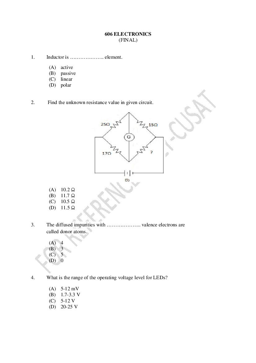
2. Find the unknown resistance value in given circuit.
(A) 10.2 Ω
(B) 11.7 Ω
(C) 10.5 Ω
(D) 11.5 Ω
3. The diffused impurities with ……………….. valence electrons are
called donor atoms.
(A) 4
(B) 3
(C) 5
(D) 0
4. What is the range of the operating voltage level for LEDs?
(A) 5-12 mV
(B) 1.7-3.3 V
(C) 5-12 V
(D) 20-25 V
Page 2
(A) 28 mW
(B) 28 W
(C) 280 mW
(D) 400 mW
6. For a MOSFET Vgs = 3 V, Ids = 5 A and Id = 2 A. Find the pinch of voltage Vp.
(A) 4.08
(B) 8.16
(C) 16.32
(D) 0
7. The crystal Oscillator frequency is very stable due to ……………….. of the Crystal.
(A) rigidity
(B) vibrations
(C) low Q
(D) high Q
8. In an LC Oscillator, if the value of L is increased four times,
the frequency of oscillations is
(A) 4f
(B) 2f
f
(C)
4
f
(D)
2
9. 2’s complement of (11001011)2 is
(A) 01010111
(B) 11010100
(C) 00110101
(D) 11100010
10. MOS families includes
(A) PMOS and NMOS
(B) CMOS and NMOS
(C) PMOS, NMOS and CMOS
(D) EMOS, NMOS and PMOS
Page 3
(A) the time taken for the output of a gate to change after the inputs have changed
(B) the time taken for the input of a gate to change after the outputs have changed
(C) the time taken for the input of a gate to change after the intermediates have
changed
(D) the time taken for the output of a gate to change after the intermediates have
changed
12. When 8051 wakes up then 0x00 is loaded to which register?
(A) DPTR
(B) SP
(C) PC
(D) PSW
13. An example of a discrete set of information/system is
(A) the trajectory of the Sun
(B) data on a CD
(C) universe time scale
(D) movement of water through a pipe
14. AM radio signal is an example for
(A) y (t ) = a × x (t )
(B) y (t ) = x1 (t ) + x2 (t )
(C) y (t ) = − x (t )
(D) y (t ) = x1 (t ) × x2 (t )
15. What provides a periodic voltage waveform?
(A) Sweep generator
(B) Voltmeter
(C) Oscillator
(D) Amplifier
16. Lumped parameter delay line consists of
(A) RC networks
(B) RL networks
(C) LC networks
(D) Resistive networks
Page 4
(A) is used for triggering the input
(B) is used for triggering the output
(C) used with time base generator
(D) used as a oscillator
18. Resistance of a metallic conductor is given by
I
(A) R=
A
ρ
(B) R=
A
ρl
(C) R=
A
l
(D) R=
A
19. Avalanche photodiodes based on HgCdTe are used for ……………….. in both the
near and far infrared.
(A) dispersion
(B) dislocation
(C) ionization
(D) array applications
20. Mechanical transducers cause
(A) power loss
(B) hysteresis loss
(C) eddy current loss
(D) frictional loss
21. Relation between temperature and resistance of a conductor is
(A) Rt =Rref [1 + t ]
(B) Rt = Rref [1 + α∆t ]
(C) Rt = Rref [1 − α t ]
(D) Rt = Rref [1 − t ]
Page 5
(A) it is cheap
(B) it is available readily
(C) it is a noble metal
(D) it gives accurate measurements
23. Reluctance of a coil is given by the relation
l
(A) S=
A
l
(B) S=
µ
a
(C) S=
µA
l
(D) S=
µA
24. Which of the following is used to establish a fixed level of
current or voltage in a transistor?
(A) Biasing
(B) Loading
(C) Load line
(D) Coupling
25. Which of the following represents common-emitter small signal input resistance?
(A) hie
(B) hfe
(C) hib
(D) hoe
26. The ear is not sensitive to ……………….. distortion.
(A) frequency
(B) amplitude
(C) harmonic
(D) phase
Page 6
(A) alpha times emitter current plus leakage current
(B) alpha times base current plus leakage current
(C) beta times emitter current plus leakage current
(D) beta times collector current plus leakage current
28. Which is NOT a basic BJT amplifier configuration?
(A) Common-drain
(B) Common-base
(C) Common-emitter
(D) Common-collector
29. The bandwidth of a single stage amplifier is ……………….. that of
multistage amplifier.
(A) equal to
(B) less than
(C) more than
(D) independent
30. Which configuration has the lowest current gain?
(A) Common-base
(B) Common-collector
(C) Common-emitter
(D) Emitter follower
31. An ammeter’s ideal resistance should be
(A) zero
(B) unity
(C) infinite
(D) the same with the circuit’s resistance
32. The input impedance of an amplifier ……………….. when negative voltage feedback
is applied.
(A) decreases
(B) becomes zero
(C) increases
(D) is unchanged
Page 7
(A) positive
(B) zero
(C) negative
(D) None of the above
34. The resistivity of a pure silicon is about
(A) 100 Ω cm
(B) 6000 Ω cm
5
(C) 3 × 10 Ω m
–8
(D) 6 × 10 Ω cm
35. When a pure semiconductor is heated, its resistance
(A) goes up
(B) goes down
(C) remains the same
(D) can’t say
36. The strength of a semiconductor crystal comes from
(A) forces between nuclei
(B) forces between protons
(C) electron-pair bonds
(D) None of the above
37. A hole in a semiconductor is defined as
(A) a free electron
(B) the incomplete part of an electron pair bond
(C) a free proton
(D) a free neutron
38. As the doping to a pure semiconductor increases,
the bulk resistance of the semiconductor
(A) remains the same
(B) increases
(C) decreases
(D) None of the above
Page 8
(A) only holes
(B) only free electrons
(C) holes and free electrons
(D) None of the above
40. In the depletion region of a p-n junction, there is a shortage of
(A) acceptor ions
(B) holes and electrons
(C) donor ions
(D) None of the above
41. A p-n junction acts as a
(A) controlled switch
(B) bidirectional switch
(C) unidirectional switch
(D) None of the above
42. The leakage current across a p-n junction is due to
(A) minority carriers
(B) majority carriers
(C) junction capacitance
(D) None of the above
43. With forward bias to a p-n junction, the width of depletion layer
(A) decreases
(B) increases
(C) remains the same
(D) None of the above
44. At absolute temperature, an intrinsic semiconductor has
(A) a few free electrons
(B) many holes
(C) many free electrons
(D) no holes or free electrons
Page 9
5 V. If a PMMC instrument is connected in parallel to this combination then the
reading of meter will be equal to
(A) 7V
(B) 5V
(C) 5.2 V
(D) 25 V
46. A PMMC instrument can be used as ammeter and as voltmeter with the help of
(A) a low resistance shunt, a low series resistance
(B) a low resistance shunt, a high series resistance
(C) a high series resistance, a low resistance shunt
(D) a low series resistance, a high shunt resistance
47. The given figure shows the Wheatstone bridge method for measurement of unknown
resistance (R). The balanced equation for Wheatstone bridge is given by
P Q
(A) =
R S
P Q
(B) =
S R
P S
(C) =
R Q
R Q
(D) =
P S
Page 10
(A) average voltage
(B) RMS voltage
(C) peak to peak voltage
(D) maximum voltage
49. If the two input waveforms are of equal amplitude and 90-degree phase difference is
applied to the CRO then the Lissajous patterns obtained will be
(A) straight line tilted at 45 degree with respect to X-axis
(B) circle
(C) ellipse
(D) vertical straight line
50. The ripple factor of a bridge rectifier is
(A) 0.482
(B) 0.812
(C) 1.11
(D) 1.21
51. A half-wave rectifier is equivalent to a
(A) a clamper circuit
(B) a clipper circuit
(C) a clamper circuit with negative bias
(D) a clamper circuit with positive bias
52. The basic reason why a full-wave rectifier has a twice the efficiency of a
half-wave rectifier is that
(A) it makes use of transformer
(B) its ripple factor is much less
(C) it utilizes both half-cycle of the input
(D) its output frequency is double the line frequency
53. A certain inverting amplifier has a closed-loop voltage gain of 25. The Op-amp has an
open-loop voltage gain of 100,000. If an Op-amp with an open-loop voltage gain of
200,000 is substituted in the arrangement, the closed-loop gain
(A) doubles
(B) drops to 12.5
(C) remains at 25
(D) increases slightly
Page 11
(A) E
(B) EF =
( Ec + Ev )
2
(C) EF =
( Ec + Ed )
2
(D) EF =
( Ev + Ea )
2
55. The drift velocity of electrons is of the order of
(A) 1 ms–1
(B) 10–3 ms–1
(C) 106 ms–1
8 –1
(D) 3 × 10 ms
56. The potential difference of an energy source that provides 50 mJ of energy for every
micro coulomb of charge that flows is
(A) 5V
(B) 50 V
(C) 500 V
(D) 50 kV
57. The example of non-ohmic resistance is
(A) copper wire
(B) carbon wire
(C) aluminium wire
(D) tungsten wire
58. The internal resistance of a cell of emf 2 V is 0.1 Ω. It is connected to a resistance of
3.9 Ω. The voltage across the cell is
(A) 0.5 V
(B) 1.95 V
(C) 1.9 V
(D) 2V
Page 12
x y in figure.
(A) ETh = 5 V; RTh = 4.5 Ω
(B) ETh = 6 V; RTh = 5 Ω
(C) ETh = 4.5 V; RTh = 10 Ω
(D) ETh = 10 V; RTh = 9 Ω
60. Two charges +3 µC and –1212 µC are separated by a distance of 0.4 m. Where should a
third change of +3 µC be placed from +3 µC so that it experiences
experiences zero force?
(A) 0.4 m
(B) 0.2 m
(C) 0.3 m
(D) 0.1 m
61. Electrons are caused to fall through a potential difference of 1500 V.
If they were initially at rest, their final speed is
3 –1
(A) 2.3 × 10 ms
7 –1
(B) 2.3 × 10 ms
(C) 4.6 × 10⁴ ms–1
(D) 0.23 × 10¹² ms–1
–
62. Two parallel metal plated maintained at a potential difference of 1000 V are
separated by 0.02 m. An electron is placed between the two plates. The force
experienced by the electron is
(A) 1.6 × 10⁻¹⁹ N
(B) 8 × 10–15 N
(C) 1000 N
(D) None of the above
Page 13
non uniform electric field. It experiences
(A) a force but no torque
(B) a force and a torque
(C) a torque but no force
(D) neither a force nor a torque
64. A circuit with a resistor, indicator and capacitor in series is resonant at frequency f 0 .
If all component values are now doubled, what is new resonant frequency?
(A) 2 f0
(B) Still f 0
f0
(C)
4
f0
(D)
2
65. The source of the magnetic field is
(A) an isolated magnetic pole
(B) static electric charge
(C) magnetic substances
(D) current loop
66. Figure shows the magnetic field around the conductor. Direction of current flowing
(A) from right to left
(B) from left to right
(C) can be either of above
(D) data incomplete
Page 14
(A) Left
(B) Right
(C) Neither left nor right
(D) Data incomplete
68. Deflection in a Galvanometer falls from 50 divisions to 20 divisions when a 12 Ω
Shunt is applied. Galvanometer resistance is
(A) 18 Ω
(B) 6Ω
(C) 9Ω
(D) 24 Ω
69. At low frequencies, the material used for transformer cores is
(A) copper
(B) silicon iron
(C) soft iron
(D) None of the above
70. The minimum relative permeability of the material can be
(A) 1
(B) slightly less than 1
(C) 0.005
(D) None of the above
71. An air-cored
cored choke is used for ……………….. applications.
(A) radio frequency
(B) audio frequency
(C) power frequency
(D) None of the above
Page 15
(A) 4H
(B) 100 H
(C) 8H
(D) None of the above
73. The magnetic energy stored in an inductor is ……………….. current.
(A) directly proportional to
(B) inversely proportional to
(C) directly proportional to square of
(D) inversely proportional to square of
74. If the frequency of the flux is increased two times, the eddy current power loss is
(A) increased two times
(B) decreased two times
(C) increased four times
(D) decreased four times
75. A sinusoidal current has a magnitude of 3 A at 120°. Its maximum value will be
(A) 3 A
3
(B) A
2
(C) 2 3 A
(D) 6 A
Page 16
(A) 70.7 V
(B) 50 V
(C) 63.7 V
(D) 100 V
77. When a 15 V square wave is connected across a 50 V a.c voltmeter, it will read
(A) 15 V
(B) 15 × 2 V
15
(C) V
2
(D) None of the above
78. A capacitor is perfect insulator for
(A) alternating current
(B) direct current
(C) direct as well as alternating current
(D) None of the above
79. Power absorbed in the pure inductive circuit is zero because
(A) reactive component of current is zero
(B) active component of current is maximum
(C) power factor of the circuit is zero
(D) reactive and active components of current cancel out
80. A pure inductor is connected to an alternating voltage source. If both the voltage and
the frequency are doubled, the circuit current
(A) becomes double
(B) is halved
(C) becomes three times
(D) no change
Page 17
op-code to be run in the program is the
(A) stack pointer
(B) program counter
(C) instruction pointer
(D) accumulator
82. The contents of the accumulator after this operation will be
MOV A,#0BH
ANL A,#2CH
(A) 11010111
(B) 11011010
(C) 00001000
(D) 00101000
83. The small extremely fast, RAM’s are called as
(A) cache
(B) heaps
(C) accumulators
(D) stacks
84. Interrupts are provided primarily as a way to
(A) improve processor utilization
(B) improve processor execution
(C) improve processor control
(D) improve processor speed
85. Mixing is used in communication to
(A) raise the carrier frequency
(B) lower the carrier frequency
(C) to altered the deviation
(D) to change the carrier frequency to any required value
86. Most of the amplification in a superhetrodyne receiver
occurs at ……………….. stage.
(A) IF
(B) RF amplifier
(C) Audio amplifier
(D) Detector
Page 18
87. In a pure inductive circuit if the supply frequency is reduced to , the current will
2
(A) be reduced by half
(B) be doubled
(C) be four times as high
(D) be reduced to one fourth
88. In a parallel R-C
C circuit, the current always ……………….. the applied voltage.
(A) lags
(B) leads
(C) remains in phase with
(D) None of the above
89. Which transistor bias circuit arrangement provides good stability using negative
feedback from collector to base?
(A) Base bias
(B) feedback bias
Collector-feedback
(C) Voltage-divider
divider bias
(D) Emitter bias
90. For full-wave
wave rectified sine wave, rms value is
(A) 0.707 im
(B) 0.6036 im
(C) 0.5 im
(D) 0.318 im
91. When transistors are used in digital circuits they usually operate in the
(A) active region
(B) breakdown region
(C) saturation and cutoff regions
(D) linear region
Page 19
(A) High voltage gain
(B) High current gain
(C) High input resistance
(D) High output resistance
93. The SI units of transconductance is
(A) Ampere Volt
(B) Volt Ampere
(C) Ohm
(D) Siemens
94. Field effect transistor’s conductivity is regulated by
(A) input current
(B) output current
(C) terminal voltage
(D) supply voltage
95. In FET, which voltage increases the channel size?
(A) Negative Vgs
(B) Positive Vgs
(C) Negative Vds
(D) Positive Vds
96. Choose the correct statement
(A) MOSFET is a unipolar, voltage controlled, two terminal device
(B) MOSFET is a bipolar, current controlled, three terminal device
(C) MOSFET is a unipolar, voltage controlled, three terminal device
(D) MOSFET is a bipolar, current controlled, two terminal device
97. Which factor determines the output voltage of an op-amp?
(A) Positive saturation
(B) Negative saturation
(C) Both positive and negative saturation voltage
(D) Supply voltage
Page 20
The value of n is
(A) 8
(B) 9
(C) 10
(D) 11
99. Decimal 43 in hexadecimal and BCD number system is
respectively ……………….. and ………………..
(A) B2 and 01000011
(B) 2B and 01000011
(C) 2B and 00110100
(D) B2 and 01000100
100. The basic storage element in a digital system is
(A) flipflop
(B) counter
(C) multiplexer
(D) encoder
101. Which device has one input and many outputs?
(A) Multiplexer
(B) Demultiplexer
(C) Counter
(D) Flipflop
102. When a differential amplifier is operated single-ended
(A) the output is grounded
(B) one input is grounded and signal is applied to the other
(C) both inputs are connected together
(D) the output is not inverted
103. For an Op-Amp, the differential gain is
(A) very high
(B) very low
(C) dependent on input voltage
(D) about 100
Page 21
(A) 90 V/µs
(B) 0.67 V/µs
(C) 1.5 V/µs
(D) None of the above
105. The input stage of an Op-amp is usually a
(A) differential amplifier
(B) class B push-pull amplifier
(C) CE amplifier
(D) swamped amplifier
106. An oscillator employs ……………….. feedback.
(A) positive
(B) negative
(C) neither positive nor negative
(D) Data insufficient
107. The piezoelectric effect in a crystal is
(A) a voltage developed because of mechanical stress
(B) a change in resistance because of temperature
(C) a change in frequency because of temperature
(D) None of the above
108. The Barkhausen criterion for an oscillator
(A) loop gain should be unity
(B) loop gain should be less than unity
(C) the phase of a feedback signal with respect to input should be 0° or 360°
(D) Both (A) and (C)
109. An oscillator differs from an amplifier because it
(A) has more gain
(B) requires no input signal
(C) requires no d.c. supply
(D) always has the same input
Page 22
(A) transient response
(B) error response
(C) dynamic response
(D) None of the above
111. ……………….. is a part of the human temperature control system.
(A) Digestive system
(B) Perspiration system
(C) Ear
(D) Leg movement
112. ……………….. is a closed loop system.
(A) Auto-pilot for an aircraft
(B) Direct current generator
(C) Car starter
(D) Electric switch
113. Transfer function of a system is used to calculate which of the following?
(A) The order of the system
(B) The time constant
(C) The output for any given input
(D) The steady state gain
114. The relation between number of free electrons (n) in a
semiconductor and temperature (T) is
(A) n ∝ T
2
(B) n ∝ T
(C) n ∝ T
(D) n ∝ T 3 2
115. When the electrical conductivity of a semiconductor is only due to the breaking of its
covalent bonds then it is said to be
(A) donor
(B) acceptor
(C) intrinsic
(D) extrinsic
Page 23
(A) positively charged
(B) produced when Boron is added as an impurity to silicon
(C) produced when Phosphorous is added as an impurity to silicon
(D) produced when carbon is added as an impurity to germanium
117. Calculate the wavelength of radiation emitted by an LED made up of a
semiconducting material with band gap energy 2.8 eV.
(A) 2.8 Å
(B) 4.3308 Å
(C) 5548.4 Å
(D) 4430.8 Å
118. The average value of current in a half wave rectifier is
I0
(A)
π
I0
(B)
2
π I0
(C)
2
2 I0
(D)
π
119. The Value of current in the following circuit will be
(A) 0A
(B) 0.01 A
(C) 0.025 A
(D) 10 A
Page 24
120. What is the frequency of a photon having energy 2.1 × 10 J?
(A) 3.1 × 10¹³ Hz
13
(B) 4.1 × 10 Hz
(C) 5.1 × 10¹³ Hz
(D) 6.1 × 10¹³ Hz
121. Astable multivibrator operating at 150 Hz has a discharge time of 2.5 m.
Find the duty cycle of the circuit.
(A) 50%
(B) 75%
(C) 95.99%
(D) 37.5%
122. In any AC circuit always
(A) apparent power is more than actual power
(B) reactive power is more than apparent power
(C) actual power is more than reactive power
(D) reactive power is more than actual power
123. A voltage follower
(A) has a voltage gain of 1
(B) is noninverting
(C) has no feedback resistor
(D) has all of these
124. Tunnel diode is basically a junction diode with
(A) high doping in p region alone
(B) high doping in p and n regions, both
(C) high doping in n region alone
(D) low doping in both p and n regions
125. A thyristor can be used as
(A) an amplifier
(B) a resistor
(C) a switch
(D) a power source
Page 25
a capacitor (0.01 µF). This is to
(A) protect the IC from inadvertent application of high voltage
(B) prevent false triggering by noise coupled onto the pin
(C) convert the trigger input to sharp pulse by differentiation
(D) suppress any negative triggering pulse
127. Gain of non-inverting amplifier is given by G =
R1
(A) 1 +
R2
R
(B) 1− 1
R2
1 + R1
(C)
R2
R1 + R2
(D)
R2
128. Stack is also known as
(A) First in First Out Memory
(B) Flash Memory
(C) Last in First Out Memory
(D) Last in Last Out Memory
129. A Nibble is equal to ……………….. bit(s)
(A) 1
(B) 2
(C) 3
(D) 4
130. ……………….. has the unit of eV
(A) Potential difference
(B) Energy
(C) Charge
(D) Current
Page 26
(A) Kingdom
(B) Division
(C) Species
(D) Order
132. An RF signal is amplitude modulated to a depth of 100% by a sinusoidal signal.
The ratio of modulated signal power to unmodulated carrier power is
(A) 1
(B) 2
2
(C)
3
3
(D)
2
133. Which of the following characteristics of electrons determine
the current in a conductor?
(A) Drift velocity alone
(B) Thermal velocity alone
(C) Both drift velocity and thermal velocity
(D) Neither drift velocity nor thermal velocity
134. Which is the relation connecting current density ‘J ’ and conductivity σ of the
conductor, when an electric field E is applied to it?
(A) J = σ 2E
(B) J = σ E2
(C) J =σE
σ
(D) J=
E
Page 27
voltage and current in the circuit?
(A) π
π
(B)
2
π
(C)
4
π
(D)
3
136. The impedance of the series LCR circuit is
2
(A) Z = R 2 + ( X L − Xc )
R2
(B) Z= 2
( X L − Xc )
2
(C) Z = R 2 − ( X L − Xc )
2
(D) Z = R 2 × ( X L − Xc )
137. Triac is a ……………….. switch.
(A) Unidirectional
(B) Mechanical
(C) Bidirectional
(D) Omni directional
138. The p-type emitter of the UJT is ……………….. doped.
(A) lightly
(B) heavily
(C) not
(D) moderately
139. Which of the following is a common application of UJT?
(A) Amplifier
(B) Rectifier
(C) Multivibrator
(D) Sawtooth generator
Page 29
(A) 2
(B) 3
(C) 4
(D) 5
141. Longer the diameter of the wire ……………….. is its resistance.
(A) unstable
(B) higher
(C) stable
(D) lesser
142. Which following material can be used as an insulator?
(A) SiO2
(B) Si
(C) Ge
(D) Cu
143. What special type of diode capable of both oscillation and amplification?
(A) Point contact diode
(B) Junction diode
(C) Zener diode
(D) Tunnel diode
144. Which type of meter requires own power source?
(A) Voltmeter
(B) Ammeter
(C) Ohmmeter
(D) Wattmeter
145. The channel of a JFET is between the
(A) gate and drain
(B) drain and source
(C) gate and source
(D) input and output
Page 30
(A) LVDT
(B) Load cell
(C) Thermistor
(D) Carbon microphone
147. The controlling parameter in MOSFET is
(A) Vds
(B) Ig
(C) Vgs
(D) Is
148. The varactor displays what useful electrical property?
(A) Variable resistance
(B) Variable capacitance
(C) Variable inductance
(D) Variable frequency
149. PIN diode is used as
(A) Amplifier
(B) Voltage controlled attenuator
(C) Rectifier
(D) None of the above
150. Potential difference between x and y
(A) 4.275 V
(B) –4.275 V
(C) 4.527 V
(D) –4.527 V
Page 31
Subject Name: 606 ELECTRONICS
SI No. Key SI No. Key SI No. Key SI No. Key SI No. Key
1 B 31 A 61 B 91 C 121 D
2 A 32 C 62 B 92 D 122 A
3 C 33 C 63 B 93 A 123 D
4 B 34 B 64 D 94 C 124 B
5 A 35 B 65 D 95 B 125 C
6 B 36 C 66 B 96 C 126 B
7 D 37 B 67 B 97 C 127 C
8 D 38 C 68 A 98 C 128 C
9 C 39 C 69 B 99 B 129 D
10 C 40 B 70 B 100 A 130 B
11 A 41 C 71 A 101 B 131 C
12 C 42 A 72 C 102 B 132 D
13 B 43 A 73 C 103 A 133 A
14 D 44 D 74 C 104 B 134 C
15 A 45 B 75 C 105 A 135 D
16 C 46 B 76 C 106 A 136 A
17 C 47 A 77 A 107 A 137 C
18 C 48 C 78 B 108 D 138 B
19 D 49 B 79 C 109 B 139 D
20 D 50 A 80 D 110 A 140 B
21 B 51 B 81 B 111 B 141 D
22 D 52 C 82 C 112 A 142 A
23 D 53 C 83 A 113 C 143 D
24 A 54 C 84 A 114 D 144 C
25 A 55 B 85 D 115 C 145 B
26 A 56 D 86 A 116 B 146 A
27 A 57 B 87 B 117 D 147 C
28 A 58 B 88 B 118 A 148 B
29 C 59 D 89 B 119 B 149 B
30 A 60 A 90 B 120 B 150 B
Document Details
| Board / Org | Cochin University |
| Exam | CUSAT Common Admission Test |
| Type | Question Paper |
| Pages | 31 |
| Updated | 22 Jul 2026 |