PU CET PG 2019 Question Paper M.E._Electronics_ Communication Engg._M.Tech. Microelectronics
Finished viewing? Save it for later —
Download PU CET PG 2019 Question Paper M.E._Electronics_ Communication Engg._M.Tech. Microelectronics (PDF · 18 pages)About PU CET PG 2019 Question Paper M.E._Electronics_ Communication Engg._M.Tech. Microelectronics
PU CET PG 2019 Question Paper M.E._Electronics_ Communication Engg._M.Tech. Microelectronics is available here for free download. Published by Punjab University for PU CET PG, this question paper can be viewed online or downloaded as a PDF (18 pages). Candidates preparing for PU CET PG can use PU CET PG 2019 Question Paper M.E._Electronics_ Communication Engg._M.Tech. Microelectronics to understand the exam pattern, the type of questions asked, and the overall difficulty level.
Frequently Asked Questions
How can I download PU CET PG 2019 Question Paper M.E._Electronics_ Communication Engg._M.Tech. Microelectronics?
Open this page and click the Download button to save PU CET PG 2019 Question Paper M.E._Electronics_ Communication Engg._M.Tech. Microelectronics as a PDF. It is completely free on AglaSem Docs.
Is PU CET PG 2019 Question Paper M.E._Electronics_ Communication Engg._M.Tech. Microelectronics free to download?
Yes. PU CET PG 2019 Question Paper M.E._Electronics_ Communication Engg._M.Tech. Microelectronics can be viewed online and downloaded as a PDF free of cost on AglaSem Docs.
How many pages does PU CET PG 2019 Question Paper M.E._Electronics_ Communication Engg._M.Tech. Microelectronics have?
PU CET PG 2019 Question Paper M.E._Electronics_ Communication Engg._M.Tech. Microelectronics contains 18 pages, which you can read online or download together as a single PDF.
Where can I find more PU CET PG study material?
You can find more PU CET PG question papers, sample papers, syllabus, and answer keys on AglaSem Docs.
PU CET PG 2019 Question Paper M.E._Electronics_ Communication Engg._M.Tech. Microelectronics – Text
Read the full text of this question paper below — useful to quickly search, copy and reference the content online without downloading the PDF.
📄 View text version (18 pages)
Page 1
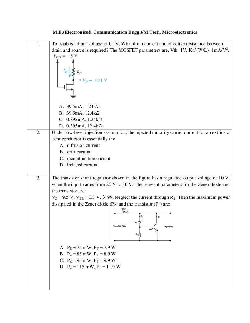
1. To establish drain voltage of 0.1V. What drain current and effective resistance between
drain and source is required? The MOSFET parameters are, Vth=1V, Kn’(W/L)=1mA/V2.
A. 39.5mA, 1.24kΩ
B. 39.5mA, 12.4kΩ
C. 0.395mA, 1.24kΩ
D. 0.395mA, 12.4kΩ
2. Under low-level injection assumption, the injected minority carrier current for an extrinsic
semiconductor is essentially the
A. diffusion current
B. drift current
C. recombination current
D. induced current
3. The transistor shunt regulator shown in the figure has a regulated output voltage of 10 V,
when the input varies from 20 V to 30 V. The relevant parameters for the Zener diode and
the transistor are:
VZ = 9.5 V, VBE = 0.3 V, β=99. Neglect the current through RB. Then the maximum power
dissipated in the Zener diode (PZ) and the transistor (PT) are:
A. PZ = 75 mW, PT = 7.9 W
B. PZ = 85 mW, PT = 8.9 W
C. PZ = 95 mW, PT = 9.9 W
D. PZ = 115 mW, PT = 11.9 W
Page 2
V. The mode of operation of the BJT is:
A. cut-off
B. saturation
C. normal active
D. reverse active
5. An ideal sawtooth voltage waveform of frequency 500 Hz and an amplitude of 3V is
generated by charging a capacitor of 2µF in every cycle. The charging requires:
A. constant voltage source of 3 V for 1 ms
B. constant voltage source of 3 V for 2 ms
C. constant current source of 3 mA for 1 ms
D. constant current source of 3 mA for 2 ms
6. The zero bias capacitance for an abrupt pn junction is 20pF. Calculate the capacitance
when the reverse bias of -7V is applied.
A. 5.16uF
B. 51.6pF
C. 5.16pF
D. 51.6uF
7. In the TTL circuit in the figure, S2 to S0 are select lines and I7 to X0 are input lines. S0 and
X0 are LSBs. The output Y is:
A. indeterminate
B. V⨁\
Page 3
V⨁\
D. Cr(A⨁B
rrrrrrr) + C(A⨁B)
8. A Zener diode regulator in figure is to be designed to meet the specifications: IL = 10 mA,
V0 = 10 V and Vin varies from 30 V to 50 V. The Zener diode has VZ = 10 V and IZK
(knee current) = 1 mA. For satisfactory operation
A. R ≤ 1800 Ω
B. 2000 Ω≤ R≤ 2200 Ω
C. 3700 Ω≤ R≤ 4000 Ω
D. R > 4000 Ω
9. A Silicon PN junction at a temperature of 20b has a reverse saturation current of 10
pico-Amperes (pA). The reverse saturation current at 40b for the same bias is
approximately:
A. 30pA
B. 40pA
C. 50pA
D. 60pA
10. What is the wavelength of light waves in free space, if the frequency is
5 × 10¹⁴?
A. 0.6 m
B. 6 mm
C. 0.06 mm
D. 0.6 µm
11. The electron concentration in a sample of uniformly doped n-type silicon at 300K varies
linearly from 1017/cm3 at x=0 to 6 x 10¹⁶/cm3 at x = 2µm. Assume a situation that
electrons are supplied to keep this concentration gradient constant with time. If the
electronic charge is 1.6 x 10⁻¹⁹coulomb and the diffusion constant is Dn = 35 cm2/ s, the
current density in the silicon, if no electric field is present is:
A. Zero
B. -1120 A/cm2
C. +1120 A/cm2
Page 4
12. If the input to the ideal comparator shown in the figure is a sinusoidal signal of 8V (peak
to peak) without any DC component, then the output of the comparator has a duty cycle
of:
A. 1/2
B. 1/3
C. 1/6
D. 1/12
13. Consider the following assembly language program
MVI B, 87H
MOV A, B
START:JMP NEXT
MVI B, 00H
XRA B
OUT PORT 1
HLT
NEXT: XRA B
JP START
OUT PORT 2
HLTB
The expression of the above program in an 8085 microprocessor will result in:
A. an output of 87H at PORT 1
B. an output of 87H at PORT 2
C. infinite looping of program execution with accumulator data alternating between
00H and 87H
D. infinite looping of program execution with accumulator data alternating between
00H and 87H
Page 5
The input bits 0 and 1 are represented by 0 and 5V respectively. The OP AMP is ideal, but
all the resistances and the 5V inputs have a tolerance of ±10%. The specification (rounded
to the nearest multiple of 5%) for the tolerance of the DAC is:
A. ±35%
B. ±20%
C. ±10%
D. ±5%
15. Often a common-collector will be the last stage before the load; the main function(s) of
this stage is to:
A. provide voltage gain
B. provide phase inversion
C. provide a high-frequency path to improve the frequency response
D. buffer the voltage amplifiers from the low-resistance load and provide impedance
matching for maximum power transfer
16. At 300 K, for a diode current of 1 mA, a certain germanium diode requires a forward bias
of 0.1435V, whereas a certain silicon diode requires a forward bias of 0.178V. Under the
conditions stated above, the closest approximation of the ratio of reverse saturation
current in germanium diode to that in silicon diode is:
A. 1
B. 5
C. 4 x 10³
D. 8 x 10³
17. For good differentiation one must ensure the time period T of signal is related to time
constant RC as:
A. T=RC
B. T<RC
Page 6
D. T>RC
18. The measured transconductance gm of an NMOS transistor operating in the linear region is
plotted against the gate voltage VG at a constant drain voltage VD. Which of the following
figures represents the expected dependence of gm on VG?
A.
B.
C. D.
19. A Zener diode is based on the principle of:
A. Thermionic emission
B. Tunneling of charge carriers across the junction
C. Diffusion of charge carriers across the junction
D. None of the above.
20. A rectangular waveguide has dimension cm 5.0 cm ×0.1cm , its cutoff frequency for the
dominant mode is
A. 5 GHz
B. 15 GHz
C. 10 GHz
D. 20 GHz
21. The capacitance per unit length and the characteristic impedance of a lossless transmission
line are C and Zo respectively. The velocity of a travelling wave on the transmission line is
A. ZoC
B. 1/(ZoC)
C. Zo/C
Page 7
22. A transmission line of characteristic impedance 50W is terminated in a load impedance
ZL. The VSWR of the line is measured as 5 and the first of the voltage maxima in the line
is observed at a distance of λ/4 from the load. The value of ZL is:
A. 10Ω
B. 250 Ω
C. (19.23+ j46.15) Ω
D. (19.23 - j46.15) Ω
23. White Gaussian noise is passed through a linear narrow band filter. The probability
density function of the envelope of the noise at the filter output is
A. Rayleigh
B. Gaussian
C. Poisson
D. Uniform
24. The steady-state error of a feedback control system with an acceleration input becomes
finite in a
A. type 0 system
B. type 1 system
C. type 2 system
D. type 3 system
25. Consider a DC voltage source connected to a series R-C circuit. When the steady-state
reaches, the ratio of energy stored in the capacitor to the total energy supplied by the
voltage source, is equal to:
A. 0.362
B. 0.500
C. 0.632
D. 1.000
26. For the network of Fig. shown below, the maximum value of power
delivered to R is
A. 0.8 W
Page 8
C. 0.4 W
D. 1.6 W
27. From measurement of the rise time of the o/p pulse of an amplifier whose input is a small
amplitude square wave, one can estimate the following parameter of the amplifier.
A. Gain-bandwidth
bandwidth product
B. Slew-Rate
C. Upper-3-dBdB frequency
D. Lower-3-dBdB frequency
28. A negative resistance having wRxy is connected to a passive network N having driving
point impedance u ((•) as shown below. For u (•) to be positive real,
A. vwRxy v ≤ w) u (z{
(z{), ∀ {
B. vwRxy v ≤ |u (z{)|
( )|, ∀ {
C.vwRxy v ≤ |} u (z{
( {), ∀ {
D.vwRxy v ≤ ∠ u (z{)
( ), ∀ {
29. The quiescent collector current IC of a transistor is increased by changing resistances. As
a result
A. gm will not be affected
B. gm will decrease
C. gm will increase
D. gm will increase or decrease depending upo
upon bias stability.
30. Average power absorbed by purely reactive components is
A. Maximum
B. Cannot be determined
C. Zero
D. Equal to resistive elements
Page 9
8 8
mpedance parameters, u = l8
open circuit impedance 8 m are:
1−z 1+z
A. n o
1+z 1+z
1−z 1+z
B. n o
−1 + z 1 − z
1+z 1+z
C. n o
1−z 1−z
1 + z −1 1+z
D. n o
−1 − z 1 − z
32. In the following graph, the number of trees (P) and the number of cut-sets
cut (Q) are:
A. P=4, Q=6
B. P=4, Q=10
C. P=2, Q=2
D. P=2, Q=6
Page 10
RL=6.8kΩ and power supply Vcc=10V. Determine the value of VBE required to operate
transistor at VCE=3.2V and the corresponding value of current IL through RL.
A. VBE=69.8mV, IL=1mA
B. VBE=69.8mV, IL=10mA
C. VBE=690.8mV, IL =1mA
D. VBE=690.8mV, IL =10mA
34. Determine the output frequency for a frequency division circuit that contains 12 flip-flops
with an input clock frequency of 20.48MHz.
A. 10.24 kHz
B. 5 kHz
C. 30.24 kHz
D. 15 kHz
35. Correlation
A. It gives a measure of similarity between two data sequences.
B. It gives a measure of dissimilarity between two data sequences
C. A & B
D. none of above
36. A band limited signal is sampled at the Nyquist rate. The signal can be
recovered by passing the samples through
A. an RC filter
B. an envelope detector
C. a PLL
D. an ideal low-pass filter with the appropriate bandwidth
37. The peak to peak input to an 8 bit PCM coder is 2 volts. The signal power to quantization
noise power ratio (in dB) for an input of
0.5 cos {}2 is
A. 47.8
Page 11
C. 95.6
D. 99.6
38. A system is defined by its impulse response ℎ(„) = 2R …(„ − 2). The system is:
A. Stable and causal
B. Causal but not stable
C. Stable but not causal
D. Unstable and non-causal
39. The addressing mode in a microprocessor in which a register is used to hold the actual
address where the data are stored is known as:
A. Indexed Addressing Mode
B. Register Direct Addressing Mode
C. Register Indirect Addressing Mode
D. Relative Addressing Mode
40. The range of signed decimal numbers that can be represented by 6-bits 1’s complement is:
A. -31 to +31
B. -63 to +64
C. -64 to +63
D. -32 to +31
41. What memory address range is
NOT represented by chip #1 and
chip #2 in the figure. Here A0 to
A15 are the address lines and CS
means chip select
A. 0100-02FF
B. 1500-16FF
C. F900-FAFF
D. F800-F9FF
Page 12
is:
A. X + Y+ Z
B. X
C. Y
D. Z
43. Consider the sequence of 8085 instructions given bel
below:
LXI H, 9258, MOV A, M, CMA, MOV M, A
Which one of the following is performed by this sequence?
A. Contents of location 9258 are moved to the accumulator
B. Contents of location 9258 are compared with the contents of the accumulator
C. Contents of location 85
8529
29 are complemented and stored in location 8529
D. Contents of location 5892 are complemented and stored in location 5892
44. What are the minimum number of 22-to-1
1 multiplexers required to generate a 2-input
2 AND
gate and a 2-input
input Ex
Ex-OR gate?
A. 1 and 2
B. 1 and 3
C. 1 and 1
D. 2 and 2
45. Figure given below shows the internal schematic of a TTL AND
AND-OR
OR-Invert (AOI) gate.
For the inputs shown in the given figure, the output Y is:
A. 0
B. 1
Page 13
rrrr
D. V\
46. A linear system is described by the following state equation
‡ = V †(2 0 1
†(2) (2) + \ ‹(2), Œℎ)•) V = l m
−1 0
The state-transition
transition matrix of the system is
0ˆ• 2 •‰„ 2 −0ˆ• 2 •‰„ 2
A. l m B. l m
−•‰„ 2 0ˆ• 2 −•‰„ 2 −0ˆ• 2
−0ˆ• 2 −•‰„ 2 0ˆ• 2 −•‰„ 2
C. l m D. l m
−•‰„ 2 0ˆ• 2 0ˆ• 2 •‰„ 2
b
47. The voltage response of the network to unit step input is Žˆ(•) =
4(4 5145 ”)
A. Under damped
B. Over damped
C. Critically damped
amped
D. Can’t be determined
48. The feedback control system in the figure is stable.
A. for all K ≥ 0
B. only if K ≥ 1
C. only if 0 ≤ K < 1
D. only if 0 ≤ K ≤ 1
49. Which of the following points is NOT on the root locus of a system with the open-loop
open
•
(•)•(•) = (45 )(45.)
transfer function Š(• 4
A. • = −z √3 B. • = −1.5 C. • = −3 D. • = −∞ −
50. Convolution of +(2 + 5) with impulse function ‘(2 − 7)is equal to
A. +(2 − 12)
B. +(2 + 12)
C. +(2 − 2)
D. +(2 + 2)
51. A sequence +(„)) with the zz-transform
†(8) = 8 7 + 8 − 2 28 + 2 − 38 67 is applied as an input to a linear, time-invariant
time
system with the impulse response ℎ(„) = 2‘ („ − 3) where:
1, „ = 0 “
‘ („) = ’
0, ˆ2ℎ)•Œ‰•)
The output at n=4 is:
A. -6
Page 14
C. 2
D. -4
52. Which of the following points is NOT on the root locus of a system with the open-loop
•
transfer function Š(•)•(•) = 4 (45 )(45.)
A. • = −z √3
B. • = −1.5
C. • = −3
D. • = −∞
53. The autocorrelation function of a rectangular pulse of duration T is
A. a rectangular pulse of duration T
B. a rectangular pulse of duration 2T
C. a triangular pulse of duration T
D. a triangular pulse of duration 2T
54. The fastest ADC is
A. Counter type
B. Flash Type
C. Successive approximation type
D. Dual slope type
55. A differential amplifier has a differential gain of 2000 and a common mode gain of 0.2.
The CMRR in dB is equal to
A. 10000 B. 400
C. 80 D. 40
56. Determine convolution sum of two sequences x(n) = {3, 2, 1, 2} and h(n) = {1, 2, 1, 2}
A. y(n) = {3,8,8,12,9,4,4}
B. y(n) = {3,8,3,12,9,4,4}
C. y(n) = {3,8,8,12,9,1,4}
D. y(n) = {3,8,8,1,9,4,4}
57. Find two different continuous-time signals that will produce the sequence
x(n) = cos( 0.15 nπ) when sampled with a sampling frequency of 8 KHz.
A. Sine(1200πt) and Cos(17200πt)
B. Cos(1200πt) and Sine(17200πt)
C. Cos(1200πt) and Cos(17200πt)
D. Sine(1200πt) and Sine(17200πt)
58. A source of angular frequency of 1rad/sec has source impedance consisting of 1Ω
resistance in series with 1H inductance. The load that will obtain maximum power transfer
is:
A. 1Ω resistance
Page 15
C. 1Ω resistance in series with 1F capacitor
D. 1Ω resistance in parallel with 1F capacitor
59. A medium bandwidth high-gain multistage transistor amplifier can be economically
realized, if the coupling technique used between different stages is
A. DC
B. RC
C. Transformer
D. LC
60.
The Thevenin’s equivalent voltage of above circuit is:
A. VAB=7.5V
B. VAB=10V
C. VAB=5V
D. VAB=3.5V
61. Let +(2) ↔ †(z{) be Fourier Transform pair. The Fourier Transform of the signal
+(52 − 3) in terms of †(z{) is given as:
—B˜
™š
A. )6 @ † " #
– –
—B˜
™š
B. – ) @ †"– #
™š
C. – ) 6™.š . † " – #
™š
D. – ) ™.š . † " – #
62. If the Laplace transform of a signal y(t) is ›(•) = 4 (46 ), then its final value is:
A. -1
B. 0
C. 1
D. unbounded
63. A carrier is phase modulated (PM) with frequency deviation of 10kHz by a single tone
frequency of 1kHz. If the single tone frequency is increased to 2kHz, assuming that the
phase deviation remains unchanged, the bandwidth of the PM signal is:
Page 16
B. 22 kHz
C. 42 kHz
D. 44 kHz
64. The impulse response ℎ[„] of a linear time-invariant
invariant system is given by ℎ[„] = …[„ + 3] +
…[„ − 2] − 2…[„ − 7] where …[„]] is the unit step sequence. The above system is
A. stable but not causal
B. stable and causal
C. causal but unstable
D. unstable and not causal
65. Many circles are drawn in a Smith chart used for transmission liline
ne calculations. The
circles shown in the figure represent:
A. unit circles
B. constant resistance circles
C. constant reactance circles
D. constant reflection coefficient circles
66. The time base in a CRO is a
A. Rectangular Waveform
B. High frequency Sinusoidal wave waveform
C. High frequency Sawtooth waveform
D. Square waveform
67. The minimum step-sizesize required for a Delta
Delta-Modulator
Modulator operating at 32K samples/sec to
track the signal (here u(t) is the unit
unit-step function)
+(2) = 125 2œ…(2) − …(2 − 1)• + (250 − 1252)(…(2 − 1)) − …(2 − 2))
so that the slope-overload
overload is avoided, would be:
-10
A. 2
B. 2-8
C. 2-6
D. 2-4
68. In a GSM system, 8 channels can co co-exist
exist in 200 kHz bandwidth using TDMA. A GSM
based cellular operator is allocated 5 MHz bandwidth. Assuming a frequency reuse factor
Page 17
can exist in one cell is:
A. 200 B. 40
C. 25 D. 5
69. When a plane wave travelling in free-space is incident normally on a medium having Ɛr =
4.0, then the fraction of power transmitted into the medium is given by:
1 –
A. B. C. D.
ž . ”
70. Which of the following is strictly bounded?
A.
B. )
C. +
D. )
71. A transmission line is distortionless if:
A. wŸ =
¡
B. wŸ = Š
C. ŸŠ = w
D. wŠ = Ÿ
72. The impulse response h(t) of a linear time-invariant continuous time system is described
by ℎ(2) = exp(¤2)…(2) + exp(¥2)…(2 − 1), where u(t) denotes the unit step function,
and α and β are real constants. This system is stable if
A. α is positive and β is positive
B. α is negative and β is negative
C. α is positive and β is negative
D. α is negative and β is positive
73. An input voltage ¦(2) = 10√2 cos(2 + 10b ) + 10 √5 cos(22 + 10b )Ž is applied to a
series combination of resistance R = 1Ω and an inductance L=1H. The resulting steady-
state current i(t) in ampere is:
A. 10 cos(2 + 55b ) + 10 cos(22 + 10b + 2§„6 2 )
.
B. 10 cos(2 + 55b ) + 10 ¨ cos(22 + 55b ) is
C. 10 cos(2 − 35b ) + 10 cos(22 + 10b − 2§„6 2 )
.
D. 10 cos(2 − 35b ) + 10 ¨ cos(22 − 35b )
74. The region of convergence of Z-transform of the sequence
– R ” R
"”# …(„) − "–# …(−„ − 1)must be
Page 18
(A) |8| < (B) |8| >
” –
– ” ”
(C)” < |8| < – (D) – < |8| < ∞
75. The transfer function of a system is given by •(•) = . The impulse response of
4 ( 46 )
the system is: (where * denotes convolution and U(t) is a unit step function.)
A. (2 ∗ ) 6 3 )‹(2)
B. (2 ∗ ) 3 )‹(2)
C. (2. ) 6 3 )‹(2)
D. (2. ) 3 )‹(2)
Document Details
| Board / Org | Panjab University |
| Exam | PU CET PG |
| Type | Question Paper |
| Pages | 18 |
| Updated | 30 Apr 2026 |