WB SET 2018 Question Paper 2 Electronic Science
Finished viewing? Save it for later —
Download WB SET 2018 Question Paper 2 Electronic Science (PDF · 16 pages)About WB SET 2018 Question Paper 2 Electronic Science
WB SET 2018 Question Paper 2 Electronic Science is available here for free download. Published by Default for Govt Jobs Exams, this question paper can be viewed online or downloaded as a PDF (16 pages). Candidates preparing for Govt Jobs Exams can use WB SET 2018 Question Paper 2 Electronic Science to understand the exam pattern, the type of questions asked, and the overall difficulty level.
Frequently Asked Questions
How can I download WB SET 2018 Question Paper 2 Electronic Science?
Open this page and click the Download button to save WB SET 2018 Question Paper 2 Electronic Science as a PDF. It is completely free on AglaSem Docs.
Is WB SET 2018 Question Paper 2 Electronic Science free to download?
Yes. WB SET 2018 Question Paper 2 Electronic Science can be viewed online and downloaded as a PDF free of cost on AglaSem Docs.
How many pages does WB SET 2018 Question Paper 2 Electronic Science have?
WB SET 2018 Question Paper 2 Electronic Science contains 16 pages, which you can read online or download together as a single PDF.
Where can I find more Govt Jobs Exams study material?
You can find more Govt Jobs Exams question papers, sample papers, syllabus, and answer keys on AglaSem Docs.
WB SET 2018 Question Paper 2 Electronic Science – Text
Read the full text of this question paper below — useful to quickly search, copy and reference the content online without downloading the PDF.
📄 View text version (15 pages)
Page 1
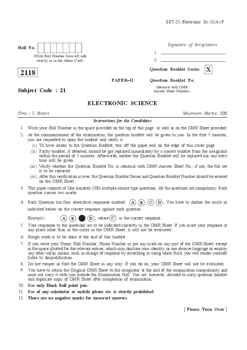
Signature of Invigilators
Roll No.
1. _______________________________
(Write Roll Number from left side
exactly as in the Admit Card) 2. _______________________________
Question Booklet Series X
2118
PAPER–II Question Booklet No.
(Identical with OMR
Subject Code : 21 Answer Sheet Number)
ELECTRONIC SCIENCE
Time : 2 Hours Maximum Marks: 200
Instructions for the Candidates
1. Write your Roll Number in the space provided on the top of this page as well as on the OMR Sheet provided.
2. At the commencement of the examination, the question booklet will be given to you. In the first 5 minutes,
you are requested to open the booklet and verify it:
(i) To have access to the Question Booklet, tear off the paper seal on the edge of this cover page.
(ii) Faulty booklet, if detected, should be got replaced immediately by a correct booklet from the invigilator
within the period of 5 minutes. Afterwards, neither the Question Booklet will be replaced nor any extra
time will be given.
(iii) Verify whether the Question Booklet No. is identical with OMR Answer Sheet No.; if not, the full set
is to be replaced.
(iv) After this verification is over, the Question Booklet Series and Question Booklet Number should be entered
on the OMR Sheet.
3. This paper consists of One hundred (100) multiple-choice type questions. All the questions are compulsory. Each
question carries two marks.
4. Each Question has four alternative responses marked: A B C D . You have to darken the circle as
indicated below on the correct response against each question.
Example: A B C D , where C is the correct response.
5. Your responses to the questions are to be indicated correctly in the OMR Sheet. If you mark your response at
any place other than in the circle in the OMR Sheet, it will not be evaluated.
6. Rough work is to be done at the end of this booklet.
7. If you write your Name, Roll Number, Phone Number or put any mark on any part of the OMR Sheet, except
in the space allotted for the relevant entries, which may disclose your identity, or use abusive language or employ
any other unfair means, such as change of response by scratching or using white fluid, you will render yourself
liable to disqualification.
8. Do not tamper or fold the OMR Sheet in any way. If you do so, your OMR Sheet will not be evaluated.
9. You have to return the Original OMR Sheet to the invigilator at the end of the examination compulsorily and
must not carry it with you outside the Examination Hall. You are, however, allowed to carry question booklet
and duplicate copy of OMR Sheet after completion of examination.
10. Use only Black Ball point pen.
11. Use of any calculator or mobile phone etc. is strictly prohibited.
12. There are no negative marks for incorrect answers.
[ Please Turn Over ]
Page 3
ELECTRONIC SCIENCE
PAPER II
1. A diode is said to be ‘ideal’ when it has 5. The Zener diode in the regulator circuit shown
(A) forward resistance = 0, Reverse resistance = in figure has a Zener voltage of 5·8 V and a Zener
and cut-in voltage = 0·7V knee current of 0·5mA. The maximum load current
(B) forward resistance = ; Reverse resistance = 0 drawn from this circuit ensuring proper functioning
and cut-in voltage = 0·7V over the input voltage range between 20 and 30 Volts, is
(C) forward resistance = 0, Reverse resistance =
Y
and cut-in voltage = 0 1K
(D) forward resistance = 0, Reverse resistance = 0 Load
Vi = 20 to 30 V
and cut-in voltage = 0
V
V z = 5·8V
2. SiO2 is a good
(A) conductor (A) 23·7 mA
(B) semiconductor (B) 14·2 mA
(C) insulator (C) 13·7 mA
(D) superconductor (D) 24·2 mA
6. Which one of the following microwave diodes
3. Assume that diodes D1 and D2 are ideal. The is suitable for very low power oscillation application
value of current (I) is only?
(A) Tunnel diode
(B) IMPATT diode
V D1
Y
2K
(C) VARACTOR diode
I (D) GUNN diode
1mA
7. In the figure, the transfer function is written as
Y 2K
V
D2
C (S ) S 4
2
R ( S ) S 7 S 13
(A) 0 mA C(S) R(S)
(B) 0·5 mA G(S) Í
+–
(C) 1 mA
(D) 2 mA
H(S) = 1
4. The modulation bandwidth of a GaAs LED is The DC gain will be | G |DC = ?
compared with that of a GaAS laser diode (LD). The 4
result is (A) | G |DC = 11
(A) LED bandwidth is greater than that of LD. 4
(B) LD bandwidth is greater than that of LED. (B) | G |DC = 9
(C) LED bandwidth is equal to the LD 2
(C) | G |DC = 3
bandwidth.
1
(D) LED bandwidth is infinitely large. (D) | G |DC = 3
Page 4
8. The Laplace transform of the -function 12. In a sinusoidal transistorized Wien-bridge
(X – a) is oscillator—
(A) 1 (A) The oscillator amplitude grows
(B) 0 monotonically until it is limited by power
a supply.
(C) e
(B) The oscillation amplitude is stabilized by
sa
(D) e a current-dependent resistance which
provides negative current feedback.
9. The Fourier transform of a -function (C) The Wein-bridge is perfectly balanced
(X – a) is given by and oscillation is obtained under this
condition.
iwa
e (D) The Barkhausen criterion is not satisfied.
(A)
2
13. In a tuned collector RF oscillator, the condition
(B) 1 of zero loop phase shift is achieved
(C) 0
(A) by a single CE transistor.
wa
(D) e (B) by the tank circuit alone which is connected
with the collector.
10. The positive values of “K” and “a”, so that the (C) by the RE — CE emitter bias of the CE
system shown in the figure oscillates at a frequency transistor.
of 2 rad/sec, are respectively (D) by the transistor amplifier and the
feedback through inductive coupling from
K ( S 1)
Í+ Í S 3 as2 2S 1 Í C(S) output to input jointly.
–
14. The OP-Amp circuit shown in the figure is
(A) 1, 0·75
(B) 2, 0·75 ideal diode
–
(C) 1, 1
(D) 2, 2
+
11. A CE p-n-p transistor amplifier with a open- Vout
Vin
loop gain of 100 and a bandwidth of 10 kHz is
operated with a negative voltage series feedback.
The feedback factor is 0·005. The bandwidth of this
amplifier with feedback applied will be X
X
(A) 10 kHz
(A) a sample/hold circuit
(B) 5 kHz
(B) a rectifier/amplifier circuit
(C) 20 kHz (C) a peak detector circuit
(D) 15 kHz (D) an analog amplifier circuit
Page 5
15. For the circuit in the figure, the value of R for 19. The value of ‘C’ required for sinusoidal osc. of
critical damping will be frequency 1kHz in the circuit of figure:
1K 2·1K
Y
Y
Y /
V+
1
F X –
– 42
Vout
+ C
(A) 10·5 ohm
(B) 6 ohm
(C) 2·5 ohm
Y
1K
(D) 3 ohm Y 1K
C
X X
16. A 2 mH inductor with some initial current can (A) 1/2 F
be represented as given in the figure, where S is the (B) 2F
Laplace transform variable. The value of initial current
1
is (C) F
2 6
(A) 0·5 Amp
(B) 2·0 Amp (D) 2 6 F
(C) 1·0 Amp
–
/
(D) 0·0 Amp 1mV
+ 20. The bandwidth of an n-stage amplifier, with
each stage having a bandwidth of B, is given by
(A) B/n
(B) B/ n
17. A transistorized astable multivibrator has
(C) B 21/N –1
(A) a single stable state.
(B) no stable state. B
(C) two stable states. (D) 1/N
2 –1
(D) infinite number of stable states.
21. A FET amplifier in CS configuration uses a
load resistance of 250 k. The ac drain resistance of
18. One of the following is incorrect related to the device is 100 k and the transconductance is
negative feedback in amplifier 0·5 mA/V. The voltage gain of the amplifier is
(A) increases the stability in amplifier. (A) 1
(B) increases the bandwidth of the amplifier. (B) –100
(C) increases the distortion in amplifier. (C) –35·7
(D) decreases the gain in amplifier. (D) 52
Page 6
22. Characteristics impedance (Z0) of an ideal 25. The output voltage (V 0) of the following
transmission line is Op-Amp circuit is
(A) Zo = LC
Y
(B) Zo = L C R1
R1
(C) Zo = L C –
V0
Y
+
(D) Zo = LC X R2
V2
Y+ Y+
R2
V1
X X X
23. One of the following is not the characteristics (A) V1 + V 2
of an ideal op-amp.
(B) V 2 – V 1
(A) Infinite slew rate
(B) Infinite input-resistance 1
(C) (V + V2)
2 1
(C) Infinite offset voltage
(D) Infinite voltage gain R1
(D) R (V1 – V 2)
2
24. The following Op-Amp circuit has parameter
values such that 2RC = 10–3 sec. The circuit will act
as
26. The following Op-Amp circuit is an active
C filter. The type of filter and its cut-off frequency are
R
Y
–
output
Y
input 18k
+
signal signal 18k
–
Y
X X X 10k
+
output
Y
X input 0·1 F
signal
(A) a differentiator for input signal frequency signal
greater than 1kHz. X
(B) an integrator for input signal frequency X
smaller than 1kHz.
X
(C) a high-pass filter with a cut-off frequency (A) High-pass, 100 rad/sec
of 1kHz. (B) Low-pass, 10000 rad/sec
(D) an integrator for input signal frequency (C) High-pass, 5000 rad/sec
greater than 1kHz. (D) Low-pass, 1000 rad/sec
Page 7
27. The ripple factor of the output waveform of a 32. A 10 bit D/A converter gives a maximum
full wave rectifier supplied by 220V, 50Hz ac at the output of 10·23V. The resolution is
input is given by (A) 5 mV
(B) 10 mV
(A) 1
3 (C) 15 mV
2
(D) 25 mV
(B) 1
4
2
33. Which of the following memory is preferred in
(C) 1
8 case of calculators?
(D) 0·81 (A) Static ROM
(B) Static RAM
28. Among the three digital IC families TTL, ECL (C) Dynamic ROM
and CMOS (D) Dynamic RAM
(A) TTL has the lowest power consumption.
(B) CMOS has the lowest noise margin. 34. The following digital circuit consists of a cascade
(C) TTL has largest fan out. of 15 XOR gates. If the input to the circuit is ‘X’ then
(D) ECL has the least propagation delay. the output F is equal to
29. Consider a 3-variable Karnaugh map using the
variables A, B and C. Which one of the following is
1
++ + + F
true if the Boolean function Y = C?
X
(A) Y = m (0, 1, 2, 3)
(B) Y = m (1, 3, 5, 7) (A) 0
(C) Y = m (2, 4, 6, 7) (B) 1
(D) Y = m (3, 4, 5, 6) (C) X
(D) X
30. In which type of shift register data is loaded in
one operation but shifted out one bit at a time?
35. The following logic symbol is that of a
(A) serial-in-parrallel-out shift register
}
(B) parallel-in-serial-out shift register D0
(C) serial-in-serial-out shift register D1 Output
Input
(D) parallel-in-parallel-out shift register D2
D3
31. In a Half Adder circuit, the sum of A and B can
be implemented using the following number of NAND S1 S2
gates
Select
(A) 3
(A) (1×4) Multiplexer
(B) 4
(B) (1×4) Demultiplexer
(C) 5 (C) Binary magnitude comparator
(D) 6 (D) Binary full adder
Page 8
36. For the following circuit, the output Y equals to 39. In the following NMOS gate circuit, the output
F is
B
+ ++++
VDD
C
D Y
+
A
A
C
A D
(A) A (C D + D)
(B) B (A+ C D) + AC
(C) C (B C + D) + AB E
B C
(D) AC + B(A + C D)
37. In the following multiplexer circuit, the Bollean
function implemented is
(A) ABCDE
I0
(B) A + B C + D E
I1
F (C) (AB + C) (D + E)
V
I2
(D) A(B + C) + DE
I3
Z
X
Y 40. The number of flip-flops required and the
(A) (0, 1, 2, 3) maximum decimal number of a MOD-15 counter is
(B) (0, 1, 3, 5) (A) 3, 15
(C) (0, 2, 4, 6) (B) 3, 14
(D) (0, 2, 4, 7) (C) 4, 15
38. A mod-3 counter is shown in figure below: (D) 4, 14
The states of the counter will be
41. The propagation delay each inverter of the
J0 Q0 J1 Q1 following ring oscillator is 5n sec. The fundamental
frequency of the oscillator output is
V
V
V
V
1 K0 Q0
1
K1 Q1
V0
clock pulse (A) 5 GHz
(A) 11 – 10 – 01 (B) 10 MHz
(B) 11 – 01 – 00
(C) 25 MHz
(C) 00 – 10 – 11
(D) 00 – 01 – 10 (D) 50 MHz
Page 9
42. Rotate instruction in microprocessor belongs 47. The signal in 8086 are in minimum mode
to when
(A) data transfer group (A) MN/MX pin is tied to VCC.
(B) arithmetic group
(B) MN/MX pin is grounded.
(C) logic group
(D) branch group (C) MN/MX pin is left open.
43. Which of the following 8085 instructions do (D) MN/MX pin is right open.
not effect CY flag?
(A) SEE M
(B) SEE R
(C) DCR M 48. The memory segment registers in 8086 are
(D) ADC M denoted by
(A) AS, BS, CS, DS
44. Consider the following program for 8085: (B) BS, CS, SS, ES
MOV A, D (C) CS, DS, SS, ES
RAL (D) DS, ES, FS, SS
MOV D, A
If initial contents of register D is decimal
number 20, the final content of register D is
(A) decimal 20
49. Which of the following is not a proper
(B) decimal 40
FORTRAN expression?
(C) decimal 10
(D) decimal 50 (A) B + A C – D
45. With (B) B + *A C
int X = 10, y = 3; (A + C)
(C) (B + D)
in usual C-program, what is the output of
modulation division in (% d, x % y)? (D) A * * (B + 2)
(A) 3
(B) 2
(C) 1
(D) 0 50. In a series regulated power supply circuit the
voltage gain Av of the “Pass” transistor satisfies the
46. Which of the following is not an interrupt line condition
is 8085?
(A) TRAP (A) Av
(B) RST 5·5 (B) 1 Av <
(C) RST 7·5 (C) Av = 1
(D) RST 9·5 (D) Av << 1
Page 10
51. What is the output of the following C-program? 55. Microwave source used for a microwave oven
is
printf(“% ·0f/n”, 3·0/4·0);
(A) reflex klystron
printf(“% ·2f/n”, 3·0/4·0);
(B) magnetron
printf(“% ·1f/n”, 3·0/4·0); (C) BWO
printf(“% ·3f/n”, 3·0/4·0). (D) IMPATT diode
(A) 1, 0·7
(B) 1, 0·75, 0·8, 0·750 56. The electric field component of an em wave is
7
(C) 0, 0·75, 1, 0·750 given by E 10 cos (10 kz ) a y V/m
(D) 0, 0·7, 0·7, 0·750 It can be inferred that
(A) the wave propagates along a y .
52. With usual begining and end of a C-program, (B) the wavelength = 188·5m.
what will be the output of the following C-program? (C) the wave number k = 0·33 rad/m.
int counter; (D) the wave attenuates as it travels.
for (counter = 10; counter > = 1;
57. Gap between two successive holes of a
– – counter) {
multihole directional coupler is
printf(“* ”);
printf(“%d”, counter); (A) g
} (B) g/4
(A) * 10 * 9 * 8 * 7 * 6 * 5 * 4 * 3 * 2 * 1 (C) g/2
(B) 10 9 8 7 6 5 4 3 2 1 (D) g/6
(C) 1 2 3 4 5 6 7 8 9 10
(D) 1 * 2 * 3 * 4 * 5 * 6 * 7 * 8 * 9 * 10 * 58. Microwave frequencies are used for
communication with deep space probes primarily
53. The critical frequency of the ionospheric layer because they do not suffer
having an electron density of 2·5 × 105/cc is (A) refraction by ionosphere.
(A) 4·5 MHz (B) attenuation in space.
(B) 45 kHz (C) velocity distortion and phase distortion.
(C) 9 MHz (D) fading.
(D) 25 MHz
59. For an IMPATT diode, which is a transit time
limited device, if the optimum operating frequency is
54. The cavity magnetron uses stropping to increased by 20%, the output mocrowave power will
(A) prevent mode jumping. (A) decrease by 20·45%
(B) prevent cathode back heating. (B) decrease by 10·14%
(C) ensure bunching. (C) increase by 35·67%
(D) improve the phase focussing effect. (D) decrease by 69·44%
Page 11
60. If the transit time through the Gunn diode be 64. The magnitude of Poynting vectors for
0·1 nsec., then the Gunn oscillation frequency will be current I flowing through a wire of length L and
(A) 0·1 GHz radius a with potential difference V between the ends
is
(B) 10 GHz
(C) 100 MHz VI
(A) S 2
(D) 1 GHz a L
61. A microwave circulator is a VI
(B) S
(A) reciprocal device. 2aL
(B) non-reciprocal device. 2
VI
(C) S
(C) when a microwave signal enters port-3, it 0 aL
emerges from port-2.
VI
(D) S L
(D) passive device which can not be converted
into a isolator by any means. 0
65. The adverse effect of noise in a communication
62. Which one of the following statements is system is maximum in
incorrect? (A) Encoder
(A) For a hollow waveguide with rectangular (B) Channel
cross-section, the dominant mode is TE10. (C) Receiver
(B) TEM mode can always propagate through (D) Source
a hollow waveguide with rectangular
cross-section. 66. Quantitization noise occurs in
(C) The cut-off wavelength for the dominant (A) PWM
mode in a hollow rectangular waveguide
is ‘2a’ where ‘a’ is the longer dimension (B) FDM
of the cross-section. (C) TDM
(D) vp · vg = c2 where vp = phase velocity and (D) PCM
vg = group velocity of the microwave
67. To generate PCM, the signal is sampled and
signal inside the hollow waveguide, ‘c’ is
converted into
the vacuum velocity of light.
(A) PWM
63. Identify which of the following expressions do (B) PPM
not correspond to Maxwell’s equations for time-
(C) PAM
varying fields.
(D) PDM
v
(A) · J 0 68. If the peak pulse power in a transmitter be
t
500 kW with a pulse width of 2 sec and the pulse
(B) · D = v repetition frequency be 1kHz then the average power
of the transmitter will be
E
(C) H ·dl E t · dS (A) 1 kW
(B) 100 kW
B (C) 1 MW
(D) · E = –
t (D) 100 W
Page 12
69. If the bandwidth of ith channel is ‘wi’ and the 73. For VSWR = 2, the reflection co-efficient
total number of channels accomodated in a time value is
interval of T is ‘N’, then the minimum bandwidth Bmin (A) = 1/2
for TDM is equal to
(B) = 1/3
N
(C) = ± 1/3
(A) N wi
i 1 (D) = ± 1/2
N
w
(B) iN 74. In a linear array of 4 centre-fed half-wave
i 1
dipole antennas excited in phase, the major lobes in
N the radiation pattern will lie
(C) wi (A) perpendicular to the line of the array.
i 1
N (B) along the line of the array.
wi
(D) 2 (C) in a direction making an angle of /4
i1 N radian with the line of the array.
(D) in a direction making an angle of 120°
70. In FDM systems used for telephone, which with the line of the array.
modulation scheme adopted?
(A) AM 75. For a 50% modulated AM signal, the ratio of
(B) DSB-SC total sideband power to carrier power at the output
(C) SSB-SC spectrum is
(D) FM (A) 1 : 4
(B) 2 : 3
71. A rectangular waveguide having TE10 mode as (C) 1 : 3
dominant mode is having a cut-off frequency of (D) 1 : 8
18GHz for TE 30 mode. The inner broad wall
dimension of the rectangular waveguide is 76. The envelope voltage of a DSB + C, AM signal
(A) 5/3 cm varies from 3 volt to 1 volt. The AM index is
(B) 5 cm (A) 33%
(C) 5/2 cm (B) 50%
(D) 10 cm (C) 40%
(D) 23%
72. A transmission line of characteristic impedance
50 is terminated in a load impedance ZL. The 77. In a superheterodyne radio receiver, the
VSWR of the line is measured as 5 and the first of the received station frequency is 800 kHz and the
voltage maxima in the line is observed at a distance intermediate frequency is 455 kHz. The local oscillator
of /4 from the load. The value of ZL is frequency should be selected as
(A) 10 (A) 1255 kHz
(B) 250 (B) 345 kHz
(C) 19·23 + j 46·15 (C) 1·71 MHz
(D) 19·23 – j 46·15 (D) 910 kHz
Page 13
78. An FM transmitter has a modulation sensitivity 83. A linear array of two half-wave dipole antennas
of 20 kHz/volt. The FM index for the 5 kHz sinsusoidal seperated by a distance of twice the wavelength of
modulation of amplitude 0·5 volt is radiation and excited in phase will have ‘n’ number
(A) 4 of lobes in the radiation field pattern where ‘n’ equals
(B) 2 to
(C) 2·5 (A) 2
(D) 10 (B) 4
79. A UJT has (C) 5
(A) stable negative resistance characteristics. (D) 8
(B) low firing current.
(C) use as a waveform generator. 84 The profile function q in the following refractive
(D) All of these characteristics. index distribution of a graded index fiber given as
80. The TRIAC can be used only in
2 r
q
2
(A) inverter n ( r ) n1 1 , r a
a
(B) rectifier
(C) multi-quadrant chopper
n1 1 2
2
, r a
(D) cycloconverter
with symbols having usual correspond to the following
81. If the core radius of a single mode optical fiber values for triangular, parabolic and step index fibers
be ‘a’, the wavelength of propagating lightwave be
respectively.
‘’, the index of refraction of the core and cladding
be n1 and n2 respectively, then the V-number of the (A) q = 1, q = and q = 2
fiber is expressed as (B) q = 1, q = 2 and q =
(C) q = 2, q = and q = 1
2a 2 2
(A) V n1 n2 (D) q = 2, q = 1 and q =
2 2 85. A pulsed laser generates 500 kW with full
2
(B) V n1 n2 width at half maximum of 10 ns at a repetition rate of
a
200 Hz. Making simplifying assumptions about pulse
2 1 power, what is the average power?
(C) V (A) 1V
a 2 2
n1 n2 (B) 1 mV
a 1 (C) 10 V
(D) V
2 2 (D) 1 nV
n1 n2
82. The total power in a Gaussian laser beam
having Io as the peak (on-axis) beam intensity and 86. What is the cut-off wavelength for the first
o as the spot size is given by higher order mode corresponding to a step-index
single mode fiber with a core diameter of 6 m and
(A) Io 2o NA = 0·12?
2 (A) 0·94 m
(B) 2 Io o
(C) 2 I o 2o (B) 2 m
(C) 1·5 m
(D) Io 2o (D) 0·5 m
Page 14
87. A laser emits a 2 mm diameter beam of highly 92. The common mode error voltage in a DVM
collimated light at a power level of 100 W. Ignoring can be eliminated by using at its input
any divergence of the beam, what is its irradiance? (A) a differential amplifier.
(A) 100 kW/m2 (B) a wideband amplifier.
(B) 50 kW/m2 (C) a turned amplifier.
(C) 63·6 kW/m2 (D) a low-pass filter.
(D) 31·8 kW/m2
93. The phenomenon of creeping occurs in
(A) Ammeter
88. One of the following is not the characteristic of
an electrical transducer: (B) Voltmeter
(A) Repeatability (C) Current meters
(B) Non-linearity (D) Ohm-meters
(C) Ruggedness
(D) Physical size 94. Which of the following meter has same
calibration for both ac and dc?
(A) Electrodynamometer type
89. Transducer for measurement of rotational (B) Moving iron type
displacement is (C) Moving coil type
(A) shaft recorder (D) Induction type
(B) differential capacitor
(C) LVDT 95. Kelvin’s double bridge is used to measure
(D) strain gauge (A) very low resistance.
(B) very high resistance.
(C) capacitor and its reactance.
90. Apart from LVDT, linear displacement can (D) inductor and its reactance.
also be sensed by
(A) RVDT
(B) capacitance transducer 96. Which one of the following gives gauge factor
of a strain gauge?
(C) thermocouple
(D) thermistor L ·R
(A)
L R
R l
(B)
91. The purpose of the synchronising control in a R l
CRO is to
R D
(A) focus the spot on the screen. (C)
R D
(B) lock the display of signal.
(C) adjust the amplitude of display. R
(D)
(D) control the intensity of the spot. R
Page 15
97. Moving coil permanent magnet instruments 99. Which one of the following characteristic
can be used for the measurement of equation can result in the stable operation of the
(A) AC and DC feedback system?
(B) AC only (A) S3 + 4S2 + S – 6 = 0
(C) DC only
(B) S3 – S2 + 5S + 6 = 0
(D) half wave rectified dc
(C) S3 + 4S2 + 10S + 11 = 0
98. A control system with a PD controller is shown (D) S4 + S3 + 2S2 + 4S + 6 = 0
in the figure. If the velocity error constant Kv = 1000
and the damping ratio = 0·5, then the values of KP
and KD are
100 C(S)
+– KP + KDS S(s10)
100. Using Routh’s criterion, the number of the
roots in the right half S-plane for characteristic equation
S4 + 2S3 + 2S2 + 3S + 6 = 0 is
(A) one
(A) KP = 100, KD = 0·09
(B) two
(B) KP = 100, KD = 0·9
(C) KP = 10, KD = 0·09 (C) three
(D) KP = 10, KD = 0·9 (D) four
Page 16
ROUGH WORK
Document Details
| Board / Org | Default |
| Exam | Govt Jobs Exams |
| Type | Question Paper |
| Pages | 16 |
| Updated | 30 Apr 2026 |