Goa Board Class 10 Question Paper 2022 Electronics
Finished viewing? Save it for later —
Download Goa Board Class 10 Question Paper 2022 Electronics (PDF · 8 pages)About Goa Board Class 10 Question Paper 2022 Electronics
Goa Board Class 10 Question Paper 2022 Electronics is available here for free download. Published by Goa Board for Class 10, this question paper can be viewed online or downloaded as a PDF (8 pages). Candidates preparing for Class 10 can use Goa Board Class 10 Question Paper 2022 Electronics to understand the exam pattern, the type of questions asked, and the overall difficulty level.
Frequently Asked Questions
How can I download Goa Board Class 10 Question Paper 2022 Electronics?
Open this page and click the Download button to save Goa Board Class 10 Question Paper 2022 Electronics as a PDF. It is completely free on AglaSem Docs.
Is Goa Board Class 10 Question Paper 2022 Electronics free to download?
Yes. Goa Board Class 10 Question Paper 2022 Electronics can be viewed online and downloaded as a PDF free of cost on AglaSem Docs.
How many pages does Goa Board Class 10 Question Paper 2022 Electronics have?
Goa Board Class 10 Question Paper 2022 Electronics contains 8 pages, which you can read online or download together as a single PDF.
Where can I find more Class 10 study material?
You can find more Class 10 question papers, sample papers, syllabus, and answer keys on AglaSem Docs.
Goa Board Class 10 Question Paper 2022 Electronics – Text
Read the full text of this question paper below — useful to quickly search, copy and reference the content online without downloading the PDF.
📄 View text version (8 pages)
Page 1
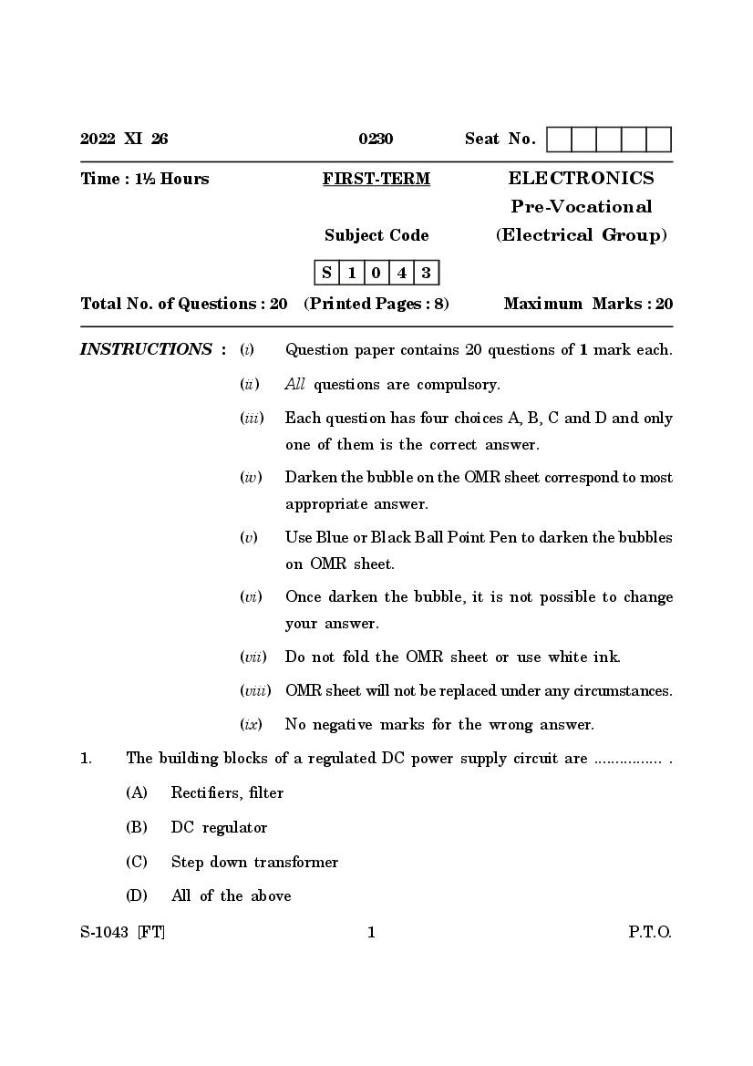
Time : 1½ Hours FIRST-TERM ELECTRONICS
Pre-Vocational
Subject Code (Electrical Group)
S 1 0 4 3
Total No. of Questions : 20 (Printed Pages : 8) Maximum Marks : 20
INSTRUCTIONS : (i) Question paper contains 20 questions of 1 mark each.
(ii) All questions are compulsory.
(iii) Each question has four choices A, B, C and D and only
one of them is the correct answer.
(iv) Darken the bubble on the OMR sheet correspond to most
appropriate answer.
(v) Use Blue or Black Ball Point Pen to darken the bubbles
on OMR sheet.
(vi) Once darken the bubble, it is not possible to change
your answer.
(vii) Do not fold the OMR sheet or use white ink.
(viii) OMR sheet will not be replaced under any circumstances.
(ix) No negative marks for the wrong answer.
1. The building blocks of a regulated DC power supply circuit are ................ .
(A) Rectifiers, filter
(B) DC regulator
(C) Step down transformer
(D) All of the above
S-1043 [FT] 1 P.T.O.
Page 2
core is .................... .
(A) To reduce hysteresis losses
(B) To reduce copper losses
(C) To reduce eddy current losses
(D) To reduce magnetic losses
3. The transformer that has same number of turns in the primary and
secondary winding is called .................... .
(A) Power Transformer
(B) Shell type Transformer
(C) Isolation Transformer
(D) Core type Transformer
4. Any complex circuit can be replaced by a single source of emf in series with
a single resistance by applying ..................... .
(A) Ohm’s law
(B) Thevenin theorem
(C) Superposition theorem
(D) Lenz’s law
5. The element suitable for doping an intrinsic semiconductor to obtain an
N-type semiconductor is ................... .
(A) Potassium
(B) Phosphorus
(C) Polonium
(D) All of the above
S-1043 [FT] 2
Page 3
voltage gain is less than unity is ..................... .
(A) Common source
(B) Common emitter
(C) Common collector
(D) Common base
7. In the following circuit, the unknown value is .................... .
(A) 120 mA
(B) 12.00 mA
(C) 1.200 mA
(D) 0.12 mA
8. The Mutual Induction between the two coils decreases when .................. .
(A) The distance between the two coils decreases
(B) When the current in the input coil increases
(C) When the number of turns in both coils is increased
(D) When the distance between the two coils is increased
S-1043 [FT] 3 P.T.O.
Page 4
because ..................... .
(A) Collector region dissipates more power
(B) Emitter region dissipates more power
(C) Collector region dissipates less power
(D) Emitter region dissipates less power
10. The AC component presents in the output voltage of the rectifier in the
power supply circuit is called ................... .
(A) Instantaneous value
(B) Ripple
(C) Amplitude
(D) Frequency
11. The disadvantege of full wave rectifier over half wave rectifier is ............... .
(A) Full wave rectifier requires more diodes than half wave rectifier
(B) Full wave rectifier requires more space than half wave rectifier
(C) Design of full wave rectifier is more complex than half wave rectifier
(D) All of the above
S-1043 [FT] 4
Page 5
(A) PNP
(B) MOSFET
(C) FET
(D) NPN
13. From the given circuit diagram of a bridge rectifier, the diodes that conducts
during the negative half cycle are ........................ .
(A) D1 and D2
(B) D2 and D3
(C) D1 and D3
(D) D2 and D4
S-1043 [FT] 5 P.T.O.
Page 6
semiconductor is ................... .
(A) 5 eV
(B) 2 eV
(C) 1 eV
(D) 0.1 eV
15. The rectification efficiency of full wave rectifier is double than half wave
rectifier because ....................... .
(A) it converts only positive cycle of AC to DC
(B) it converts only negative cycle of AC into DC
(C) it converts both positive and negative cycles of AC into DC
(D) none of the above
16. PN Junction diode allows the current to flow, when it is .................... .
(A) Reverse biased
(B) Forward biased
(C) In both forward and reverse biased
(D) None of the above
17. The heat produced in the transformer’s winding is due to ................. .
(A) Input current
(B) Input resistance
(C) Load current
(D) Load resistance
S-1043 [FT] 6
Page 7
diagram is ...................... .
(A) 10
(B) 8
(C) 100
(D) 20
19. Smitha Broke open an old power supply circuit and found that the
transformer have three terminal in its secondary windings and only two
diodes are visible. The power supply circuit most probably contains ................ .
(A) Bridge rectifier
(B) Half wave rectifier
(C) Centre tap rectifier
(D) None of the above
20. Since there are no moving parts in a transformer, it requires .................... .
(A) Extra care and maintenance
(B) Very little care and maintenance
(C) No care and maintenance
(D) All of the above
S-1043 [FT] 7 P.T.O.
Page 8
S-1043 [FT] 8
Document Details
| Board / Org | Goa Board |
| Exam | Class 10 |
| Type | Question Paper |
| Pages | 8 |
| Updated | 24 Sep 2026 |