KSET 2020 Question Paper Electronic Science
Finished viewing? Save it for later —
Download KSET 2020 Question Paper Electronic Science (PDF · 24 pages)About KSET 2020 Question Paper Electronic Science
KSET 2020 Question Paper Electronic Science is available here for free download. Published by Karnataka Exams for Karnataka State Eligibility Test, this question paper can be viewed online or downloaded as a PDF (24 pages). Candidates preparing for Karnataka State Eligibility Test can use KSET 2020 Question Paper Electronic Science to understand the exam pattern, the type of questions asked, and the overall difficulty level.
Frequently Asked Questions
How can I download KSET 2020 Question Paper Electronic Science?
Open this page and click the Download button to save KSET 2020 Question Paper Electronic Science as a PDF. It is completely free on AglaSem Docs.
Is KSET 2020 Question Paper Electronic Science free to download?
Yes. KSET 2020 Question Paper Electronic Science can be viewed online and downloaded as a PDF free of cost on AglaSem Docs.
How many pages does KSET 2020 Question Paper Electronic Science have?
KSET 2020 Question Paper Electronic Science contains 24 pages, which you can read online or download together as a single PDF.
Where can I find more Karnataka State Eligibility Test study material?
You can find more Karnataka State Eligibility Test question papers, sample papers, syllabus, and answer keys on AglaSem Docs.
KSET 2020 Question Paper Electronic Science – Text
Read the full text of this question paper below — useful to quickly search, copy and reference the content online without downloading the PDF.
📄 View text version (24 pages)
Page 1
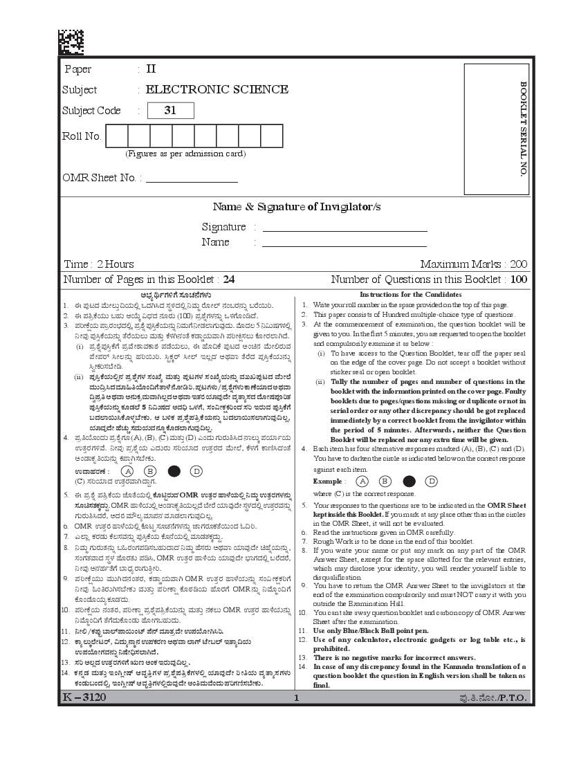
Booklet SERIAL No.
Subject : Electronic Science
Subject Code : 31
Roll No.
(Figures as per admission card)
OMR Sheet No. : ____________________
Name & Signature of Invigilator/s
Signature : _________________________________
Name : _________________________________
Time : 2 Hours Maximum Marks : 200
Number of Pages in this Booklet : 24 Number of Questions in this Booklet : 100
A»Ü¦ìWÜÚWæ ÓÜãaÜ®æWÜÙÜá Instructions for the Candidates
1. D ±Üâo¨Ü ÊæáàÆᤩ¿áÈÉ J¨ÜXst ÓܧÙܨÜÈÉ ¯ÊÜá¾ ÃæãàÇ… ®ÜíŸÃÜ®Üá° ŸÃæÀáÄ. 1. Write your roll number in the space provided on the top of this page.
2. D ±Ü£ÅPæ¿áá ŸÖÜá BÁáR Ë«Ü¨Ü ®ÜãÃÜá (100) ±ÜÅÍæ°WÜÙÜ®Üá° JÙÜWæãíw¨æ. 2. This paper consists of Hundred multiple-choice type of questions.
3. ±ÜÄàPæÒ¿á ±ÝÅÃÜí»Ü¨È
Ü É, ±ÜÅÍæ° ±ÜâÔ¤P¿
æ á®Üá° ¯ÊÜáWæ ¯àvÜÇÝWÜáÊÜâ¨Üá. Êæã¨ÜÆ 5 ¯ËáÐÜWÜÙÜÈÉ 3. At the commencement of examination, the question booklet will be
¯àÊÜâ ±ÜâÔ¤Pæ¿á®Üá° ñæÃæ¿áÆá ÊÜáñÜᤠPæÙÜX®Üíñæ PÜvÝx¿áÊÝX ±ÜÄàQÒÓÜÆá PæãàÃÜÇÝX¨æ. given to you. In the first 5 minutes, you are requested to open the booklet
(i) ±ÜÅÍæ°±ÜâÔ¤PæWæ ±ÜÅÊæàÍÝÊÜPÝÍÜ ±Üvæ¿áÆá, D Öæã©Pæ ±Üâo¨Ü Aíb®Ü ÊæáàÈÃÜáÊÜ and compulsorily examine it as below :
±æà±ÜÃ… ÔàÆ®Üá° ÖÜÄÀáÄ. ÔrPÜRÃ… ÔàÇ… CÆÉ¨Ü A¥ÜÊÝ ñæÃæ¨Ü ±ÜâÔ¤Pæ¿á®Üá° (i) To have access to the Question Booklet, tear off the paper seal
on the edge of the cover page. Do not accept a booklet without
ÔÌàPÜÄÓܸæàw.
sticker seal or open booklet.
(ii) ±ÜâÔ¤Pæ¿áÈÉ®Ü ±ÜÅÍæ°WÜÙÜ ÓÜíTæ ÊÜáñÜᤠ±ÜâoWÜÙÜ ÓÜíTæ¿á®Üá° ÊÜááS±Üâo¨Ü ÊæáàÇæ
(ii) Tally the number of pages and number of questions in the
ÊÜáá©Åst ÊÜÞ×£Áãí©Wæ ñÝÙæ ®æãàwÄ. ±ÜâoWÜÙÜá/±ÜÅÍæ°WÜÙÜá PÝOæ¿Þ¨Ü A¥ÜÊÝ
booklet with the information printed on the cover page. Faulty
©Ì±ÜÅ£ A¥ÜÊÝ A®ÜáPÜÅÊÜáÊÝXÆÉ¨Ü A¥ÜÊÝ CñÜÃÜ ¿ÞÊÜâ¨æà ÊÜÂñÝÂÓÜ¨Ü ¨æãàÐܱÜäÄñÜ booklets due to pages/questions missing or duplicate or not in
±ÜâÔ¤Pæ¿á®Üá° PÜãvÜÇæ 5 ¯ËáÐÜ¨Ü AÊܘ JÙÜWæ, ÓÜíËàPÜÒPÜÄí¨Ü ÓÜÄ CÃÜáÊÜ ±ÜâÔ¤PæWæ serial order or any other discrepancy should be got replaced
Ÿ¨ÜÇÝÀáÔPæãÙÜÛ¸æàPÜá. B ŸÚPÜ ±ÜÅÍ氱ܣÅPæ¿á®Üá° Ÿ¨ÜÇÝÀáÓÜÇÝWÜáÊÜâ©ÆÉ, immediately by a correct booklet from the invigilator within
¿ÞÊÜâ¨æà ÖæaÜác ÓÜÊÜá¿áÊÜ®Üã° PæãvÜÇÝWÜáÊÜâ©ÆÉ. the period of 5 minutes. Afterwards, neither the Question
4. ±ÜÅ£Áãí¨Üá ±ÜÅÍæ°WÜã (A), (B), (C) ÊÜáñÜᤠ(D) Gí¨Üá WÜáÃÜá£Ô¨Ü ®ÝÆáR ±Ü¿Þì¿á Booklet will be replaced nor any extra time will be given.
EñܤÃÜWÜÚÊæ. ¯àÊÜâ ±ÜÅÍæ°¿á G¨ÜáÃÜá ÓÜÄ¿Þ¨Ü EñܤÃÜ¨Ü ÊæáàÇæ, PæÙÜWæ PÝ~Ô¨Üíñæ 4. Each item has four alternative responses marked (A), (B), (C) and (D).
AívÝPÜꣿá®Üá° PܱݳXÓܸæàPÜá. You have to darken the circle as indicated below on the correct response
E¨ÝÖÜÃÜOæ : A B C D against each item.
(C) ÓÜÄ¿Þ¨Ü EñܤÃÜÊÝX¨ÝªWÜ. Example : A B C D
5. D ±ÜÅÍæ° ±Ü£ÅPæ¿á hæãñæ¿áÈÉ PæãqrÃÜáÊÜ OMR EñܤÃÜ ÖÝÙæ¿áÈÉ ¯ÊÜá¾ EñܤÃÜWÜÙÜ®Üá° where (C) is the correct response.
ÓÜãbÓÜñÜPÜR¨Üáª. OMR ÖÝÙæ¿áÈÉ AívÝPÜꣿáÆÉ¨æ ¸æàÃæ ¿ÞÊÜâ¨æà Óܧ٨
Ü È
Ü É EñܤÃÊ
Ü ®Ü áÜ ° 5. Your responses to the questions are to be indicated in the OMR Sheet
WÜáÃÜá£Ô¨ÜÃæ, A¨ÜÃÜ ÊÜåèÆÂÊÜÞ±Ü®Ü ÊÜÞvÜÇÝWÜáÊÜâ©ÆÉ. kept inside this Booklet. If you mark at any place other than in the circles
6. OMR EñܤÃÜ ÖÝÙæ¿áÈÉ Pæãor ÓÜãaÜ®æWÜÙÜ®Üá° hÝWÜÃÜãPÜñæÀáí¨Ü K©Ä. in the OMR Sheet, it will not be evaluated.
6. Read the instructions given in OMR carefully.
7. GÇÝÉ PÜÃÜvÜá PæÆÓÜÊÜ®Üá° ±ÜâÔ¤Pæ¿á Pæã®æ¿áÈÉ ÊÜÞvÜñÜPÜR¨Üáª.
7. Rough Work is to be done in the end of this booklet.
8. ¯ÊÜá¾ WÜáÃÜáñÜ®Üá° Ÿ×ÃÜíWܱÜwÓÜŸÖÜá¨Ý¨Ü ¯ÊÜá¾ ÖæÓÜÃÜá A¥ÜÊÝ ¿ÞÊÜâ¨æà bÖæ°¿á®Üá°, 8. If you write your name or put any mark on any part of the OMR
ÓÜíWÜñÜÊÝ¨Ü ÓܧÙÜ ÖæãÃÜñÜá ±ÜwÔ, OMR EñܤÃÜ ÖÝÙæ¿á ¿ÞÊÜâ¨æà »ÝWܨÜÈÉ ŸÃæ¨ÜÃæ, Answer Sheet, except for the space allotted for the relevant entries,
¯àÊÜâ A®ÜÖÜìñæWæ ¸Ý«ÜÂÃÝWÜᣤàÄ. which may disclose your identity, you will render yourself liable to
9. ±ÜÄàPæÒ¿áá ÊÜááX¨Ü®ÜíñÜÃÜ, PÜvÝx¿áÊÝX OMR EñܤÃÜ ÖÝÙæ¿á®Üá° ÓÜíËàPÜÒPÜÄWæ disqualification.
¯àÊÜâ ×í£ÃÜáXÓܸæàPÜá ÊÜáñÜᤠ±ÜÄàPÝÒ PæãsÜw¿á ÖæãÃÜWæ OMR®Üá° ¯Êæã¾í©Wæ 9. You have to return the OMR Answer Sheet to the invigilators at the
end of the examination compulsorily and must not carry it with you
Pæãívæã¿áÂPÜãvܨÜá. outside the Examination Hall.
10. ±ÜÄàPæÒ¿á ®ÜíñÜÃÜ, ±ÜÄàPÝÒ ±ÜÅÍ氱ܣÅPæ¿á®Üá° ÊÜáñÜᤠ®ÜPÜÆá OMR EñܤÃÜ ÖÝÙæ¿á®Üá° 10. You can take away question booklet and carbon copy of OMR Answer
¯Êæã¾í©Wæ ñæWæ¨ÜáPæãívÜá ÖæãàWÜŸÖÜá¨Üá. Sheet after the examination.
11. ¯àÈ/PܱÜâ³ ¸ÝÇ…±ÝÀáíp… ±æ®… ÊÜÞñÜÅÊæà E±ÜÁãàXÔÄ. 11. Use only Blue/Black Ball point pen.
12. PÝÂÆáRÇæàoÃ…, ˨Üá®ݾ®Ü E±ÜPÜÃÜ| A¥ÜÊÝ ÇÝW… pæàŸÇ… CñÝ©¿á 12. Use of any calculator, electronic gadgets or log table etc., is
E±ÜÁãàWÜÊÜ®Üá° ¯Ðæà˜ÓÜÇÝX¨æ. prohibited.
13. There is no negative marks for incorrect answers.
13. ÓÜÄ AÆÉ¨Ü EñܤÃÜWÜÚWæ Má| AíPÜ CÃÜáÊÜâ©ÆÉ .
14. In case of any discrepancy found in the Kannada translation of a
14. PܮܰvÜ ÊÜáñÜᤠCíXÉàÐ… BÊÜ꣤WÜÙÜ ±ÜÅÍ氱ܣÅPæWÜÙÜÈÉ ¿ÞÊÜâ¨æà Äࣿá ÊÜÂñÝÂÓÜWÜÙÜá question booklet the question in English version shall be taken as
PÜívÜáŸí¨ÜÈÉ, CíXÉàÐ… BÊÜ꣤WÜÙÜÈÉÃÜáÊÜâ¨æà Aí£ÊÜáÊæí¨Üá ±ÜÄWÜ~ÓܸæàPÜá. final.
K – 3120 1 ±Üâ.£.®æãà./P.T.O.
Page 2
Paper – II
Note : This paper contains Hundred (100) objective type questions. Each question carries
two (2) marks. All questions are compulsory.
1. Which of the following material is 5. nMOS devices are formed in a
class II-VI compound ? (A) n-substrate with heavy doping
(A) AlAs (B) GaN level
(C) CdS (D) InP (B) n-substrate with moderate doping
level
2. Which of the following compound will
(C) p-substrate with heavy doping
have highest break down voltage ?
level
(A) GaP (B) GaAs
(D) p-substrate with moderate doping
(C) Si (D) Ge level
3. Intrinsic electron concentration in a
6. In the circuit given below, the power
semiconductor is given by dissipated by the 3 ohm resistor is
(A) ni = Nce– (Ec – Ei)/kT
(B) ni = Nce (Ec – Ei)/kT
(C) ni = Nc/e (Ec + Ei)/kT
(D) ni = EcEi/Nce–(Ec – Ei)/kT
Where Nc is effective density of states, (A) 2 W (B) 4 W
Ec is energy level of conduction band
(C) 8 W (D) 12 W
and Ei is average energy.
4. Because of ___________, TEM cannot 7. If the Laplace transform of a function
be used to study live cells. 1
is F(s) = , then its initial value is
(A) high vacuum s+2
(A) 0
(B) high temperature
(B) ( 12 )
(C) high humidity (C) 1
(D) high energy X-rays (D) 2
Paper II 2 K-3120
Page 3
unit circle in the z-plane, then the largest
a look-up table is found by XLAT
possible phase change that the system
can introduce is instruction of 8086 microprocessor by
(A) Mπ (B)
( Mπ2 ) adding the contents of
(C) ( 2πM ) (D) 2 Mπ (A) DS, AL, BX
9. What is the efficiency of series fed class (B) AL, BX
‘A’ amplifier ?
(C) AX, BX
(A) 25% (B) 50%
(C) 78.5% (D) Above 90% (D) DS, AX, BX
10. The charge amplifiers are normally used
for amplifying signals from 14. Signal on ALE pin of 8086
(A) Photo transistor
microprocessor is high means
(B) Piezoelectric transducer
(C) Hall effect devices (A) Multiplexed address/data bus
(D) Optical encoders contains address information
11. Advanced schotty is a part of (B) Multiplexed address/data bus
(A) ECL family (B) CMOS family contains data information
(C) TTL family (D) FET family
(C) Lower 16 lines of multiplexed
12. Positive logic in a circuit is one in
which : address/data bus contains address
(A) Logic 0 and 1 are represented by 0 information and remaining 4 lines
and positive voltage respectively
contains status information
(B) Logic 0 and – 1 are represented
by negative and positive voltage (D) Lower 16 lines of multiplexed
respectively
address/data bus contains data
(C) Logic 0 voltage level is higher than
logic 1 voltage level information and remaining 4 lines
(D) Logic 0 voltage level is lower than contains status information
logic 1 voltage level
K-3120 3 Paper II
Page 4
8051 microcontroller is included in the process of reception ?
(A) Encoding
(A) Increment stack by 2 and store 16 bit
(B) Decoding
content to address pointed to by SP
(C) Storage
(B) Decrement stack by 1 and store 8 bit
(D) Interpretation
content to address pointed to by SP
19. In AM if carrier of 100 percent modulated
(C) Increment stack by 1 and store 8 bit wave is suppressed, the percentage
content to address pointed to by SP power saving will be
(D) Store 8 bit content to address pointed (A) 50 (B) 66.66
to by SP and then increment stack (C) 150 (D) 100
by 1 20. How many roots of the given characteristic
equation are/is in RHS of S-plane
16. A directional coupler with 3 or more s3 – 4s2 + s + 6 = 0 ?
holes is preferred to two pole coupler. (A) 0 (B) 2
(A) To reduce spurious mode (C) 3 (D) 4
generation
21. A second order system subjected to
(B) To increase coupling of the signal a step input has a response whose
maximum overshoot is 50%. Then the
(C) Because it is more efficient system may be said to be
(D) To increase the bandwidth of the (A) Overdamped
system (B) Critically damped
(C) Underdamped
17. If transmission bandwidth is doubled in
(D) Undamped
FM, SNR is
22. For a string voltage of 3300 V, let there be
(A) Doubled
six series connected SCRs each of voltage
(B) Raised by four times 600 V. then the string efficiency is
(C) Decreased by four times (A) 91.7% (B) 96%
(C) 98.54% (D) 99.36%
(D) Halved
Paper II 4 K-3120
Page 5
making a LED
following
a) GaAs b) GeInSb
(A) Quantum noise c) AlSi d) InGaN
Codes :
(B) Ramp voltage error (A) a, c
(C) Step size error (B) a, b
(C) a, c, d
(D) Speed limitation (D) a, d
27. Following are the active sources
24. A pulse wave is ‘ac’ coupled to an a) Fluorescent lamp
oscilloscope with Ri = 10 MΩ and b) L C D
Cc = 0.1 µF, what is the longest pulse c) L E D
d) Silicon diode
width (or space width) that can be
Codes :
displayed without noticeable low- (A) c
frequency distortion being introduced (B) b, c
by oscilloscope ? (C) a, c
(D) b, c, d
(A) 10 ms (B) 30 ms 28. Which of the following statements are true ?
(C) 75 ms (D) 100 ms a) Bipolar transistors are not used in
BiCMOS circuits
b) Bipolar transistors have superior
25. The reference level control in a spectrum transconductance characteristics
than MOS transistors
analyser is used to adjust the amplitude c) The current per unit area
characteristics of MOS transistors
of a main signal (or reference signal) to are superior than Bipolar
transistors
(A) Fill the screen vertically
d) The Bipolar transistors have better
switching performance than MOS
(B) Adjust the centre frequency transistors
Codes :
(C) Normalize the range of frequency
(A) a and c are true
(D) Synchronize with tracking (B) a and d are true
generator (C) b and c are true
(D) b and d are true
K-3120 5 Paper II
Page 6
true for XRD ? true with respect to the FIR systems ?
a) It is not suitable for the physical a) The systems have finite impulse
characterization of liquids response
b) It is not suitable for the physical b) The systems have infinite impulse
response
characterization of polymers
c) The systems are recursive
c) In the XRD plot, the x-axis represents
angle d) The systems are non-recursive
d) In the XRD plot, the x-axis represents Codes :
distance (A) a and c are true
Codes : (B) b and c are true
(A) b and c are true (C) b and d are true
(B) a and c are true (D) a and d are true
(C) a and d are true 32. Following are the ideal characteristics
of op-amp
(D) b and d are true
a) High output impedance
30. For an even and half-wave symmetry
b) High open loop gain
function, the Fourier coefficients are
c) High input bias current
a) ao = 0 b) an = 0
d) High slew rate
c) bn = 0 d) ao ≠ 0
Which of the above statements are true ?
Codes :
Codes :
(A) a and b are true
(A) d
(B) a and c are true (B) b, c
(C) b and c are true (C) b, d
(D) c and d are true (D) b, c, d
Paper II 6 K-3120
Page 7
power supply is initiated by following = ∑ (2, 3, 4, 5, 13, 15) + ∑ d (8, 9, 10, 11)
components is given below, where ‘d’ is don’t care
a) v = b′c + ad
a) External pass transistor
b) v = b′c + ad + a′ b c′
b) A zener diode
c) v = b′c + a′d
c) Current sense resistor d) v = b′c′ + ad
d) error amplifier Which of the above is true ?
Codes : Codes :
(A) a and c
(A) b
(B) b only
(B) a, b, d
(C) a and d
(C) a, b, c (D) d only
(D) b, c, d 36. Which of the following statements is/are
true with respect to TEST pin of 8086
34. Following are Boolean properties
microprocessor ?
a) x + y = y + x a) If low, execution continues else
microprocessor is in wait state
b) xy = yx
b) If high, execution continues else
c) x + (yz) = (x + y) (x + z) microprocessor is in wait state
d) x (y + z) = xy + xz c) It is used to test the status of
co-processor
Which of the above are commutative
d) It is used to test the status of
properties ?
memory
Codes : Codes :
(A) c and d (A) a
(B) a and b (B) a and c
(C) a and d
(C) a and c
(D) b and d
(D) b and d
K-3120 7 Paper II
Page 8
microcontroller can be addressed as a a) Wider bandwidth due to higher
byte only ? frequencies
a) PCON b) TMOD b) Smaller component size leading to
smaller systems
c) IE d) TCON
c) Existence of low signal losses
Codes :
d) Lower interference due to lower
(A) a, b and c signal crowding
(B) a and c Which of these advantages are present
(C) c and d in RF/Microwave system applications :
Codes :
(D) a and b
(A) b, c and d
38. Consider the following statements for (B) a, c and d
a square waveguide of cross section
(C) a, b and d
3 m × 3m, it has been found that
(D) a, b and c
a) at 6 GHz dominant mode will
propagate 40. Consider the following statements
b) at 6 GHz all the modes are a) Spectral density express average
evanescent power in a waveform as a function
of frequency
c) at 11 GHz only dominant modes
b) Role of channel in communication
and no higher order mode will
system is mixing of signals
propagate
c) For providing two or more voice
d) at 7 GHz degenerate modes will circuits on same carrier we use
propagate DSB – SC
Which of the above statements are correct ? d) Notch filter is a band stop filter
Codes : Codes :
(A) a and b (A) a and d
(B) a, b and d (B) a and b
(C) b and c
(C) b and c
(D) b and d
(D) b, c and d
Paper II 8 K-3120
Page 9
a) Forward error correction can be controlled by
code corrects error without a) Changing the supply frequency
retransmission of signal
b) Changing the supply voltage
b) Read solomon codes are non-
binary c) Inserting resistance in rotor circuit
c) A feedback decoder makes a hard- d) Various ways of cascade
decision connection
d) Maximum distance is related to the Codes :
error correcting capability of the
(A) a and b
codes
(B) c and d
Choose the correct answer from above :
Codes : (C) a, b and c
(A) b and c (D) a and d
(B) a and c 44. Consider the following statements
(C) a and b associated with electrical/electronic
(D) b and d transducers
a) Mass-inertia effects are minimised
42. A minimum phase transfer function
b) These transducers consume very
a) Does not have poles or zeros in the
little power
right half of S-plane
c) The response time is large
b) Does not have poles or zeros on
the jw-axis, excluding the origin d) Transmission and processing
c) Does not have poles or zeros in the the signal for the purpose of
left-half of S-plane measurement are easier
d) Does have poles or zeros on the Which of the above are correct for
jw-axis electrical/electronic transducers ?
Codes : Codes :
(A) a and d (A) a, b and c
(B) a and b (B) b, c and d
(C) c and d (C) a, c and d
(D) b and c
(D) a, b and d
K-3120 9 Paper II
Page 10
following medical application emission color
a) Muscle contraction List – I List – II
b) Grip force a. InGaN i. Green
c) Heart wall motion b. Gap : N ii. IR
d) Finger contact pressure c. GaAs iii. Red
Codes : d. AlGaAs iv. Blue
Codes :
(A) a, c
a b c d
(B) a, d
(A) iii ii i iv
(C) a, b, d
(B) iv ii iii i
(D) b, c, d
(C) iv i ii iii
46. Match the following : (D) iii i ii iv
List – I List – II 48. Match List – I (Layer information in
nMOS design) with List – II (stick
a. LED i. Indirect bandgap
diagram color coding)
b. Silicon Diode ii. Passive device
List – I List – II
c. Candle iii. Current injection
a. N-diffusion i. Red
d. LCD iv. Spontaneous
b. Polysilicon ii. Green
emission c. Implant iii. Black
Codes : d. Contact area iv. Yellow
a b c d Codes :
(A) iv i ii iii a b c d
(B) iii i iv ii (A) i ii iii iv
(C) iv ii iii i (B) ii i iv iii
(D) ii iii i iv (C) iii i iv ii
(D) iv iii i ii
Paper II 10 K-3120
Page 11
process) with List – II (Suitable
fabrication process) List – I (Y – parameters) with List – II
List – I List – II
a. Annealing i. Physical vapor
deposition
b. Metalization ii. Oxidation
c. SiO2 iii. Chemical vapor
deposition
d. Epitaxy iv. Rapid thermal
processing
Codes :
a b c d List – I List – II
(A) i ii iii iv
a. Y11 i. s + 1
(B) ii iii iv i
(C) iv i ii iii b. Y12 ii. – 1
(D) i iv iii ii
c. Y22 + Y21 iii. 1 + 1
50. Match List – I (Network theorems) with s
List – II (Salient features of theorems)
d. Y22 iv. s
List – I List – II
a. Superposition i. Open-circuited
theorem voltage source Codes :
b. Thevenin’s ii. Short-circuited
theorem current source a b c d
c. Norton’s iii. Scaling and
theorem additive property (A) iii ii iv i
d. Maximum iv. Power delivered
power to load
transfer (B) i iv ii iii
theorem
Codes : (C) iii iv ii i
a b c d
(D) i ii iv iii
(A) iv iii i ii
(B) iii ii i iv
(C) ii iv i iii
(D) iii i ii iv
K-3120 11 Paper II
Page 12
List – I List – II List – I List – II
a. Class A i. Non-linear
amplifier distortion a. In multiple i. due to different
synchronous logic path
b. Class C ii. Cross over
amplifier distortion sequential
c. Class B iii. Low distortion elements
amplifier
b. In multiple ii. skew present
d. Class AB iv. Low power
synchronous problem
amplifier
sequential
Codes :
elements
a b c d
(A) iv ii i iii c. skew in iii. at low clock
(B) iii ii i iv clock occurs speed skew
(C) iv i ii iii while rarely
(D) ii i iii iv distribution is trouble some
53. Match the following : d. When iv. skew refers
sequential to phase shift
List – I List – II
elements between
a. CMRR i. 6 dB/decade operates at rectangular
b. roll-off ii. 120 dB maximum clock waveform
c. Open-loop iii. 0.5 V/µs clock frequency
gain
d. Slew rate iv. 20,000 Codes :
Codes : a b c d
a b c d (A) iii iv ii i
(A) iv i ii iii
(B) iv iii i ii
(B) ii i iv iii
(C) iv iii i ii (C) i ii iii iv
(D) ii iii iv i (D) ii i iii iv
Paper II 12 K-3120
Page 13
with R/M bits of instruction template.
List – I List – II
List – I List – II
a. Excitation i. State variable
table is a changes that a. MOV AL, [BX] i. 000
occurs as a b. MOV AL, [BX + DI] ii. 001
sequential circuit
c. MOV AL, iii. 110
change states
[BX + SI + 5678H]
b. State table ii. Tabular
d. MOV AL, [FA64H] iv. 111
is a representation
of the state Codes :
changes that a b c d
occurs in
(A) i ii iii iv
sequential
circuits (B) ii i iii iv
c. Transition iii. Table that (C) iv ii i iii
table is a specifies the (D) iv i iii ii
excitation values
for each state 57. Match the following lists with respect
variable to registers and their address in 8051
micro controller.
d. State diagram iv. Graphical
is a representation List – I List – II
of the interaction a. IP i. 80H
of state transition
under different b. PSW ii. B8H
input c. A iii. DOH
conditions d. PO iv. EOH
Codes : Codes :
a b c d a b c d
(A) ii iii iv i (A) iii ii i iv
(B) ii i iv iii (B) ii iii iv i
(C) iii i ii iv (C) ii iii i iv
(D) iii ii i iv (D) iii ii iv i
K-3120 13 Paper II
Page 14
List – I List – II List – I List – II
a. Cavity wave meter i. Microwave a. Directional i. improvement
coupler of stability
component
and efficiency
b. Magic Tee ii. Microwave
is achieved by
source strapping
c. VSWR iii. Microwave b. Rectangular ii. Detect the
frequency waveguide presence of
measurement both forward
and backward
d. Magnetron iv. Reflection
waves in a
coefficient
waveguide
measurement
c. Magnetron iii. TE10
Codes :
d. Reciprocity iv. Antenna
a b c d theorem measurements
(A) iii i ii iv Codes :
a b c d
(B) iii i iv ii
(A) ii iii iv i
(C) i iii ii iv
(B) i iii iv ii
(D) iii ii iv i
(C) ii iii i iv
(D) iii ii iv i
Paper II 14 K-3120
Page 15
List – I List – II List – I List – II
a. Cross talk i. reduce a. L{f(t – a)u(t – a)} i. F1(s) F2(s)
scattering loss
t
b. L ∫ f1 (τ) f2 (t − τ)dτ ii. F(s + a)
b. Immune to ii. Optical fibre 0
RFI
c. Cladding iii. Copper cable c. L{f1(t). f2 (t)} iii. e–as F(s)
d. Elastic plastic iv. Mechanical d. L {f(t) e–at} iv. F1(s) * F2(s)
material isolation Codes :
Codes : a b c d
a b c d (A) ii iv i iii
(A) iii ii iv i (B) iii iv i ii
(B) iii ii i iv (C) i iii ii iv
(C) iii i ii iv (D) iii i iv ii
(D) iii iv ii i
63. Match the following :
61. Match the following :
List – I List – II
List – I List – II a. Thyrister i. High speed
a. Shot noise i. ambient light application
b. Dark noise ii. leakage current b. MOSFET ii. Small on-state
drop
c. Surface dark iii. statistical
noise nature c. IGBT iii. Slow devices
d. Amplifier iv. minimum as d. BJT iv. Large on-state
noise possible drop
Codes : Codes :
a b c d a b c d
(A) iii i ii iv (A) iii ii i iv
(B) iii ii i iv (B) iii ii iv i
(C) ii i iv iii (C) iii iv ii i
(D) ii i iii iv (D) ii iv i iii
K-3120 15 Paper II
Page 16
List – I List – II the resistivity of these materials in
a. Piezoelectric i. Passive device increasing order
transducer
a) Bakelite
b. Stain gauge ii. Voltage source
c. Thermo iii. Current device b) Mica
couple
c) Pure silica
d. Photo iv. Built in
transistor amplification d) Window glass
Codes : Codes :
a b c d
(A) a, d, b, c
(A) iv i ii iii
(B) ii iv i iii (B) c, b, d, a
(C) iii ii i iv (C) a, b, c, d
(D) iii i ii iv
(D) c, a, b, d
65. Match the following transducers :
List – I List – II 67. The sequence of steps used in the
a. Hot wire i. Dialysate flow fabrication of gate structure in nMOS
in artificial transistor is
kidney
b. Venturi ii. Blood flow in a) Thin oxide deposition
arteries b) Polysilicon deposition
c. Turbine iii. Respiratory gas
flow c) Photoresist deposition and etching
d. Electromagnetic iv. Blood flow in d) Thick oxide deposition on
lung-heart
machines p-substrate
Codes : Codes :
a b c d
(A) a, c, d, b
(A) ii iii iv i
(B) i iii iv ii (B) b, d, c, a
(C) iii i iv ii (C) d, c, a, b
(D) iii iv i ii
(D) a, b, c, d
Paper II 16 K-3120
Page 17
processes are used in analog-to-digital FPGA in order of data propagation from
conversion system is input to output
a) Coding a) Pull up stage
b) Sampling b) Input/output block
c) Prefiltering c) Switching matrix
d) Quantization d) Configurable logic block
Codes :
Codes :
(A) b, a, c, d
(A) b, c, a, d
(B) a, d, b, c
(B) b, c, d, a
(C) c, d, a, b
(C) a, b, c, d
(D) c, b, d, a
(D) a, b, d, c
69. Following are different types of voltage
71. Arrange the following flags of 8086
regulators
microprocessor in the order of their
a) Emitter follower
appearance in flag register from MSB
b) Zener diode to LSB
c) Op-amp regulator a) Overflow flag
d) 3-pin IC b) Trap flag
Arrange them in the increasing order c) Direction flag
of load regulation.
d) Interrupt flag
Codes :
Codes :
(A) b, a, c, d
(A) a, b, d, c
(B) b, a, d, c
(B) b, c, d, a
(C) a, b, d, c
(C) b, d, c, a
(D) a, b, c, d
(D) a, c, d, b
K-3120 17 Paper II
Page 18
a) FM appearance in SMPS of mobile phone
charger from input to output
b) 100% AM
a) High frequency rectifier
c) 10% AM
d) 50% AM b) Switching transistor
Arrange the power input to Antenna c) Transformer
in increasing order. d) High voltage rectifier
Codes : Codes :
(A) a, c, d, b (A) a, b, c, d
(B) b, d, c, a
(B) d, b, c, a
(C) a, d, c, b
(C) a, c, b, d
(D) b, c, d, a
(D) d, b, a, c
73. Consider the following :
75. Arrange the following blocks in the
a) F D M
order of their signal flow in a spectrum
b) T D M analyser
c) O F D M a) Detector
d) O A M b) Verticle amplifier
Arrange above terms in order of
c) IF amplifier
bandwidth efficiency and spectral
efficiency. d) Mixer
Codes : Codes :
(A) b, a, d, c (A) d, c, a, b
(B) b, a, c, d (B) a, c, d, b
(C) a, b, c, d (C) c, a, b, d
(D) a, b, d, c (D) d, a, c, b
Paper II 18 K-3120
Page 19
The following items consist of two statements, resistance.
one labelled as “Assertion (A)” and the
Reason (R) : In pinch-off region, drain
other labelled as “Reason (R)”. You have to
current becomes constant.
examine the two statements carefully and decide
if the Assertion (A) and the Reason (R) are 78. Assertion (A) : In P-well CMOS circuit,
individually true and if so whether the reason deep p-well diffusion is created.
is a correct explanation of the Assertion.
Reason (R) : Deep p-well is used in p-well
Select your answer to these items using the
CMOS to achieve higher threshold
codes given below and mark your answer
voltage.
accordingly.
79. Assertion (A) : Ion implantation is a
Codes :
useful alternative to high temperature
(A) Both (A) and (R) are true and (R) is
diffusion.
the correct explanation of (A)
Reason (R) : The advantage of ion
(B) Both (A) and (R) are true, but (R) is
implantation is that it can be carried out
not the correct explanation of (A)
at low temperature without disturbing
(C) (A) is true, but (R) is false
previous diffusion region.
(D) (A) is false, but (R) is true
80. Assertion (A) : Z-parameters can be
76. Assertion (A) : An N-type semiconductor used to test the reciprocity property of
behaves as an intrinsic semiconductor at
two-post network.
very high temperature.
Reason (R) : A two-post network is said
Reason (R) : The braking of the
to be reciprocal if the 2-parameters of the
covalent bonds becomes a significant
network satisfy the condition Z11 = Z22.
phenomenon at high temperature.
K-3120 19 Paper II
Page 20
transfer theorem is used to find the power stage does not exhibit a low, constant
delivered to the load of the network. output impedance in both logic states.
Reason (R) : Maximum power is Reason (R) : In DTL when output transistor
delivered to the load if the load resistance is saturated, the output impedance is low
value is equal to the 50% of the source and when output transistor is cut-off, the
resistance value. output impedance is parallel equivalent
of the pull-up resistor.
82. Assertion (A) : Instrumentation amplifier
have very high CMRR. 86. Assertion (A) : CISC architecture gives
Reason (R) : Instrumentation amplifier more emphasis on Hardware.
has two identical op-amps at input in Reason (R) : CISC processor contains
non-inverting mode. complex instructions with variable length.
83. Assertion (A) : A simple low pass filter 87. Assertion (A) : Microcontroller application
can be used as integrator. requires the counting of external events or
Reason (R) : Combination of RC gives the generation of precise internal time
linear characteristic for the integrator. delay.
Reason (R) : 8051 microcontroller is
84. Assertion (A) : Under parallel types A/D
having two timer/counters.
conversion, a flash convertors, the input
is simultaneously compared with various 88. Assertion (A) : Electromagnetic
reference voltages which are one LSB oscillations are sustained in a two-cavity
apart. Klystron due to feedback of output power
Reason (R) : Characteristics of flash to the input cavity in proper phase.
convertors is very low speed conversion Reason (R) : Two-cavity Klystron is
is possible. since the speed is only limited the most suitable microwave source at
by switching time of the comparators laboratory to generate local oscillations
and gates. for frequency measurements.
Paper II 20 K-3120
Page 21
electron effect for production of RC series circuit in parallel with SCR.
Microwaves. Reason (R) : Voltage across a capacitor
Reason (R) : Gun diode has the negative can not change instantaneously.
resistance characteristic.
94. Assertion (A) : Potentiometers cannot
90. Assertion (A) : Stimulated emission be used as error detectors in position
gives rise to light amplification in control systems.
LASER cavity. Reason (R) : The number of turns of a
potentiometer places an upper limit on
Reason (R) : Metastable energy state in
its accuracy.
material cavity gives rise to stimulated
emission. 95. Assertion (A) : Load cell is a compound
transducer.
91. Assertion (A) : Plastic fibers are used in
short distance application. Reason (R) : Strain gauge is used in
load cell.
Reason (R) : Plastic fibers offers
substantially lower attenuation than Based on the following paragraph answer
glass fibers. Q. No. 96-100.
92. Assertion (A) : Stability of a system The Fourier transform is used for the
deteriorates when integral control is frequency analysis of discrete-time aperiodic
incorporated in it. finite energy signals. But the Fourier transform
of a discrete-time aperiodic signal is a
Reason (R) : With integral control action
continuous function of frequency and it is not
order of the system increases and higher
computationally convenient representation.
the order of the system, the more the
To overcome this problem, frequency domain
system tends to become unstable.
sampling of Fourier transform is carried out.
K-3120 21 Paper II
Page 22
of the a periodic discrete-time signal is called
the Discrete Fourier Transform (DFT). DFT (A) Real and odd
plays an important role in the implementation (B) Real and even
of many signal processing algorithms. The
DFT satisfies many important properties like (C) Imaginary and odd
linearity, periodicity etc. The Inverse Discrete
Fourier Transform (IDFT) is used to transform (D) Imaginary and even
the signal from frequency domain to time
domain.
99. If DFT{x(n)} = x(k) and DFT {y(n)} =
y(k) then which of the following is the
96. The Fourier transform x(ω) of an
aperiodic sequence x(n) is given by valid Parseval’s theorem expression ?
∞
N −1 N −1
(A) X (ω ) = ∑ x(n)e -jωn (A) ∑ x( n)y∗ ( n) =∑ X( k)Y∗ ( k)
n = −∞ n =0 k =0
1 ∞
(B) X (ω ) = ∑
∞ ∞
x(n)e -jωn
2 π n = −∞ (B) ∑ x( n ) y ∗ ( n ) = ∑ X ( k ) Y ∗ ( k )
n =−∞ k =−∞
N-1
(C) X (ω ) = ∑ x(n)e -jωn N −1 ∞
(C) ∑ x( n)y ( n) =N ∑ X( k)Y ( k)
∗ ∗
n=0
n =0 k =−∞
N-1
1
(D) X (ω ) = ∑ x(n)e -jωn
2π n = 0 N −1
1 N −1
(D) ∑ N ∑ X( k)Y ( k)
∗ ∗
x ( n ) y ( n ) =
n =0 k =0
97. The IDFT of
X(k) = {6, –2 + j2, –2, –2 – j2} is 100. If DFT {x(n)} = {12, – 4 + j4, – 4, – 4 – j4}
then the DFT {x((n – 3))4} is
(A) {2, 3, 4, 1}
(A) {12, – 4 – j4, 4, – 4 + j4}
(B) {2, 6, 0, 2}
(B) {12, – 4 + j4, – 4, – 4 – j4}
(C) {0, 1, 2, 3}
(C) {12, – 2 + j2, 4, – 2 – j2}
(D) {3, 6, 2, 1} (D) {12, – 2 + j3, – 4, –2 – j3}
Paper II 22 K-3120
Page 23
K-3120 23 Paper II
Page 24
Paper II 24 K-3120
Document Details
| Board / Org | Karnataka Exams |
| Exam | Karnataka State Eligibility Test |
| Type | Question Paper |
| Pages | 24 |
| Updated | 24 Sep 2026 |