CUSAT CAT 2021 Question Paper Electronics
Finished viewing? Save it for later —
Download CUSAT CAT 2021 Question Paper Electronics (PDF · 32 pages)About CUSAT CAT 2021 Question Paper Electronics
CUSAT CAT 2021 Question Paper Electronics is available here for free download. Published by Cochin University for CUSAT Common Admission Test, this question paper can be viewed online or downloaded as a PDF (32 pages). Candidates preparing for CUSAT Common Admission Test can use CUSAT CAT 2021 Question Paper Electronics to understand the exam pattern, the type of questions asked, and the overall difficulty level.
Frequently Asked Questions
How can I download CUSAT CAT 2021 Question Paper Electronics?
Open this page and click the Download button to save CUSAT CAT 2021 Question Paper Electronics as a PDF. It is completely free on AglaSem Docs.
Is CUSAT CAT 2021 Question Paper Electronics free to download?
Yes. CUSAT CAT 2021 Question Paper Electronics can be viewed online and downloaded as a PDF free of cost on AglaSem Docs.
How many pages does CUSAT CAT 2021 Question Paper Electronics have?
CUSAT CAT 2021 Question Paper Electronics contains 32 pages, which you can read online or download together as a single PDF.
Where can I find more CUSAT Common Admission Test study material?
You can find more CUSAT Common Admission Test question papers, sample papers, syllabus, and answer keys on AglaSem Docs.
CUSAT CAT 2021 Question Paper Electronics – Text
Read the full text of this question paper below — useful to quickly search, copy and reference the content online without downloading the PDF.
📄 View text version (32 pages)
Page 1
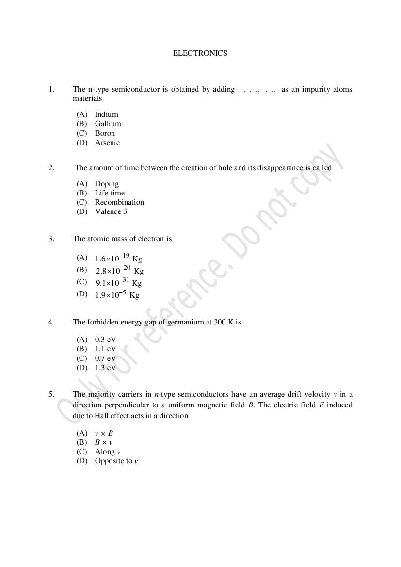
1. The n-type semiconductor is obtained by adding …………… as an impurity atoms
materials
(A) Indium
(B) Gallium
(C) Boron
(D) Arsenic
2. The amount of time between the creation of hole and its disappearance is called
(A) Doping
(B) Life time
(C) Recombination
(D) Valence 3
3. The atomic mass of electron is
(A) 1.6 1019 Kg
(B) 2.8 1020 Kg
(C) 9.11031 Kg
(D) 1.9 105 Kg
4. The forbidden energy gap of germanium at 300 K is
(A) 0.3 eV
(B) 1.1 eV
(C) 0.7 eV
(D) 1.3 eV
5. The majority carriers in n-type semiconductors have an average drift velocity v in a
direction perpendicular to a uniform magnetic field B. The electric field E induced
due to Hall effect acts in a direction
(A) v×B
(B) B×v
(C) Along v
(D) Opposite to v
Page 2
valance and conduction bands?
(A) Wood
(B) Plastic
(C) Gold
(D) Germanium
7. The value of the ripple factor in an half-wave rectifier is
(A) 1.21
(B) 0.42
(C) 0.21
(D) 1.42
8. FET is a
(A) Positive resistance device
(B) Negative resistance device
(C) Current controlled device
(D) Voltage controlled device
9. The expression that gives the relationship between and β of BJT is
1
(A)
1
(B)
1
(C)
1
(D)
1
10. How many electrons are there in the 4th orbit of Germanium atom?
(A) 4
(B) 8
(C) 16
(D) 32
Page 3
(A) 40.6 %
(B) 81.2 %
(C) 90.2 %
(D) 51.4%
12. The three band colour code of 12 kilo ohm resistor is
(A) Black Orange Red
(B) Red Brown Orange
(C) Black Brown Red
(D) Brown Red Orange
13. The equivalent capacitance value of two capacitors of 10 micro Farad
each connected in parallel is
(A) 5 micro Farad
(B) 10 micro Farad
(C) 20 micro Farad
(D) 40 micro Farad
14. At high frequencies, ordinary diodes don’t work properly because of
(A) forward bias
(B) reverse bias
(C) breakdown
(D) charge storage
15. The capacitive reactance value of a 10 micro farad capacitor for
a DC current is
(A) 0
(B) 10
(C) 20
(D) Infinity
16. Which of the following processes is preferred to from
the gate dielectric (SiO2) of MOSFET?
(A) Sputtering
(B) Wet oxidation
(C) Molecular beam epitaxy
(D) Dry oxidation
Page 4
a center-tap full wave rectifier is
(A) Vm 2
(B) Vm
(C) 2Vm
(D) 4Vm
18. The transistor parameter independent dc biasing circuit is
(A) Fixed biasing
(B) Collector feedback biasing
(C) Emitter Follower biasing
(D) Voltage-divided biasing
19. The biasing conditions for the transistor to use as an amplifier is
(A) Emitter-base junction should be in forward biased and collector-base junction
should be in reverse biased
(B) Emitter-base junction should be in reverse bias and collector-base junction
should be forward biased
(C) Both emitter-base junction and collector-base junction should be forward
biased
(D) Both emitter-base junction and collector-base junction should be reverse biased
20. The phase difference between the input and output voltages of a CE amplifier is
(A) 0°
(B) 90°
(C) 180°
(D) 270°
21. The oscillator circuit that gives stable oscillations is
(A) LC oscillators
(B) RC oscillators
(C) Crystal oscillators
(D) RLC oscillators
Page 5
the sustained oscillations of an oscillator circuit is
(A) A 1 and total phase around the loop is 0°
(B) A 1 and total phase around the loop is 0°
(C) A 1 and total phase around the loop is 180°
(D) A 0 and total phase around the loop is 0°
23. Cutoff frequency of first order Butterworth filter is
1
(A)
2 6RC
RC
(B)
2 RC
1
(C)
2 RC
1
(D)
2 RC
24. In a series resonant circuit, if X C and X L are the capacitive and inductive
reactances respectively, which of the following condition is true at resonance?
(A) XC X L
(B) XC X L
(C) XC X L
(D) X C 10 X L
25. If L and f indicate inductance value and frequency,
the expression for the inductive reactance X L is
(A) fL
1
(B)
fL
(C) 2 fL
1
(D)
2 fL
Page 6
Bipolar Junction Transistor (BJT) inactive region in a linear circuit
(i) The emitter diode must be forward biased
(ii) The collector diode must be reverse biased
(iii) The voltage across the collector diode must be greater than the breakdown
voltage
(iv) The voltage across the collector diode must be less than the breakdown voltage
(A) (i), (ii) and (iii) only
(B) (i), (iii) and (iv) only
(C) (i), (ii) and (iv) only
(D) (i), (ii), (iii) and (iv)
27. In a network with the voltage source and resistances, the maximum power is
transformed to a load if
(A) The load resistance is equal to zero
(B) The load resistance is equal to infinity
(C) The load resistance is equal to source resistance
(D) The load resistance is equal to half of the source resistance
28. Output impedance and CMRR of an ideal op-amp
are …………… and …………… respectively.
(A) ∞ and 0
(B) ∞ and ∞
(C) 0 and 0
(D) 0 and ∞
29. The CMMR of an operational amplifier is defined as
(A) The ratio of differential voltage gain to common-mode voltage gain
(B) The ratio of common mode voltage gain to differential voltage gain
(C) Ratio of the offset voltage to offset current
(D) Sum of the common-mode voltage gain to differential voltage gain
30. The feedback element in an op-amp integrator is
(A) Resistor
(B) Capacitor
(C) Inductor
(D) Transistor
Page 7
feedback circuit, then the frequency of oscillations given by
1
(A) f
2 RC
(B) f 2 RC
1
(C) f
RC
(D) f RC
32. The output waveform of a differentiator with the square waveform input is
(A) Sinusoid
(B) Square
(C) Triangular
(D) Spike
33. A 555 time is configured to generate the square waveform.
Then the duty cycle of the output waveform is
(A) 25%
(B) 50%
(C) 75%
(D) 100%
34. An oscillator is an amplifier with …………… feedback.
(A) Positive
(B) Negative
(C) Both Positive and Negative
(D) No
35. Closed loop voltage gain of a non-inverting operational amplifier with a feedback
resistor 10 kilo ohms and a series resistor of 10 kilo ohms is equal to
(A) 1
(B) 2
(C) 10
(D) 20
Page 8
(A) AND gate
(B) OR gate
(C) NAND gate
(D) NOT gate
37. In a digital logic family, the full form for TTL is
(A) Tristate Transistor Logic
(B) Total Transistor Logic
(C) Transfer Transistor Logic
(D) Transistor Transistor Logic
38. The desirable feature of an instrumentation amplifier is
(A) Low output impedance
(B) High output impedance
(C) Low input impedance
(D) Zero input impedance
39. In CRO saw tooth voltage is applied at the
(A) Cathode
(B) Accelerating anode
(C) Vertical deflection plates
(D) Horizontal deflection plates
40. Semiconductor strain gauges employ …………… property to measure strain.
(A) Piezoresistive
(B) Thermo-electric
(C) Diffusion
(D) Drift
41. Anemometers are used to measure …………… parameter.
(A) velocity
(B) volume
(C) density
(D) temperature
Page 9
(A) LVDT
(B) RVDT
(C) Thermistor
(D) Diaphragms
43. The Hall sensor senses
(A) temperature
(B) humidity
(C) magnetic field
(D) pressure
44. The resistance of LDR …………… when exposed to radiant energy.
(A) increases
(B) decreases
(C) reaches maximum
(D) remains unaltered
45. In an amplifier circuit, the coupling capacitor is used to
(A) block dc current
(B) block ac current
(C) dc biasing the amplifier
(D) increase the bandwidth of an amplifier
46. Efficiency of Class A Power amplifier is
(A) 25%
(B) 50%
(C) 75%
(D) 90%
47. Half power bandwidth is also known as
(A) 3 dB bandwidth
(B) +3 dB bandwidth
(C) +2 dB bandwidth
(D) 2 dB bandwidth
Page 10
and the wavelength of the electromagnetic wave is given by
(A) f c
(B) c f
(C) f2 c
(D) c2 f
49. A current of 2.0 A passes through a cell of e.m.f 1.5 V having internal resistance of
0.15 Ω. There potential difference across the terminals of the cell is
(A) 1.35 V
(B) 1.00 V
(C) 1.50 V
(D) 1.20 V
50. In an AM wave, useful power is carried by
(A) Carrier
(B) Sidebands
(C) both sidebands and carrier
(D) neither carrier nor sidebands
51. A networks contains liner resistors and idle voltage sources. If values of all the
resistor are doubled, then the voltage across each resistor is
(A) halved
(B) doubled
(C) increased by four times
(D) not change
52. The condition AD – BC = 1 for a two port network implies that the network is a
(A) Reciprocal network
(B) Lumped element network
(C) Lossless network
(D) Unilateral element network
Page 11
(A) FM demodulation
(B) PM demodulation
(C) AM demodulation
(D) FSK demodulation
54. The total average power in a sinusoidal AM wave with a carrier power of 10 watt and
the modulation index of 0.5 is equal to
(A) 10.25 watts
(B) 11.25 watts
(C) 102.5 watts
(D) 112.5 watts
55. The modulation index of an FM wave for a maximum frequency deviation
of 50 kilo Hertz and the modulating frequency of 5 kilo Hertz is
(A) 5
(B) 10
(C) 15
(D) 250
56. Which statement is true with the Frequency Modulation?
(A) Noise immunity is better than AM
(B) It covers wider area than AM
(C) The FM modulator circuit is simpler than AM modulator circuit
(D) The bandwidth requirement of FM is less than AM
57. In an AM, the carrier signal used in the modulation process is
(A) pulse
(B) sinusoidal
(C) square
(D) triangular
Page 12
(i) z11 = z22
(ii) y21 = y12
(iii) h21 = h12
(iv) AD – BC = 0
(A) (i) and (ii)
(B) (ii) and (iii)
(C) (iii) and (iv)
(D) (iv) and (i)
59. Norton’s theorem states that a complex network connected to a load
can be replaced with an equivalent impedance
(A) In series with a current source
(B) In parallel with a voltage source
(C) In series with a voltage source
(D) In parallel with a current source
60. The distance of a geostationary satellite from the surface of the earth is nearly
(A) 360 Km
(B) 3600 Km
(C) 36000 Km
(D) 360000 Km
61. The unit of flux density is
(A) MMF
(B) Weber
(C) Maxwell
(D) Tesla
62. In an n channel JFET, the gate is
(A) n type
(B) p type
(C) Metal
(D) Insulator
Page 13
(A) Negative feedback improves stability and system response
is less sensitive to external inputs and parameter variations
(B) Feedback does not affect stability and system response is
sensitive to disturbances and parameter variations
(C) Negative feedback affects stability and system response is
more sensitive disturbances and parameter variations
(D) None of the above
64. The Gray code for the binary digit 10110 is
(A) 11101
(B) 10101
(C) 11001
(D) 10011
65. The output of an AND gate with three inputs A, B and C is HIGH for
(A) A = 0, B = 0, C = 0
(B) A = 1, B = 1, C = 1
(C) A = 1, B = 0, C = 1
(D) A = 0, B = 1, C = 1
66. The number of select lines used in 1:16 de-multiplexer is
(A) 2
(B) 4
(C) 8
(D) 16
67. A decade counter is a
(A) Mod-2 counter
(B) Mod-3 counter
(C) Mod-5 count
(D) Mod-10 counter
Page 14
(A) commutative law
(B) associative law
(C) identity law
(D) distributive law
69. The 4-variable Karnaugh map has …………… number of cells.
(A) 4
(B) 8
(C) 16
(D) 32
70. Number of flip-flops required for the divide by 8 ripple counter is
(A) 2
(B) 3
(C) 4
(D) 8
71. Among the digital logic families, the highest power dissipating one is
(A) TTL
(B) PMOS
(C) NMOS
(D) ECL
72. The storage element in a static RAM is
(A) Diode
(B) Resistor
(C) Capacitor
(D) Flip-flop
73. In random access memory
(A) Data can be written only once
(B) Data can be read only once
(C) Data can be written only once but data can be read many times
(D) Data can be written and read many number of times
Page 15
(A) Electrical Programmable Read Only Memory
(B) Electronic Programmable Read Only Memory
(C) Electromagnetic Programmable Read Only Memory
(D) Erasable Programmable Read Only Memory
75. The binary 2’s complement equivalent of 5 is
(A) 0101
(B) 1011
(C) 1010
(D) 0111
–2t
76. The Laplace transform of e sin 2𝜔t is
2s
(A)
( s 2)2 2 2
2w
(B)
( s 2)2 4 2
2s
(C)
( s 2)2 4 2
2s
(D)
( s 2)2 2 2
77. In a circuit shown below, the value of Thevenin’s voltage and resistance
across the terminals A and B are
(A) 10 V and 20 ohm
(B) 10 V and 16.6 ohm
(C) 6.6 V and 16.6 ohm
(D) 6.6 V and 10 ohm
Page 16
(A) 10 V
(B) 60 V
(C) 100 V
(D) 150 V
79. The RC circuit shown below behaves like a
(A) All-pass filter
(B) High-pass filter
(C) Band-pass filter
(D) Low-pass filter
80. The value of output voltage in the circuit shown below is
(A) 5V
(B) 10 V
(C) 15 V
(D) 20 V
Page 17
According to the sample theorem, the sampling frequency which is not valid is
(A) 5 KHz
(B) 12 KHz
(C) 15 KHz
(D) 20 KHz
82. The Fourier transform of a voltage signal x(t ) is X ( f ). The unit of X ( f ) is
(A) volt
(B) volt-sec
(C) volt/sec
2
(D) volt
83. If a signal f (t) has energy E, the energy of the signal f (2t) is equal to
(A) E
(B) E 2
(C) 2E
(D) 4E
84. The autocorrelation function of an energy signal has
(A) No symmetry
(B) Odd symmetry
(C) Conjugate symmetry
(D) Even symmetry
85. The amplitude spectrum of a Gaussian pulse is
(A) uniform
(B) A sine function
(C) Gaussian
(D) An impulse function
Page 18
from an earth station via an uplink to a satellite, amplified in a transponder on board
the satellite and then transmitted via a downlink to another earth station. The most
popular frequency band for satellite communication is
(A) 16 MHz for the uplink and 14 MHz for the downlink
(B) 4 GHz for the uplink and 6 GHz for the downlink
(C) 6 GHz for the uplink and 4 GHz for the downlink
(D) 10 GHz for the downlink and 8 GHz for the uplink
87. Boosting of higher frequency at the transmitter is done by using
(A) De-emphasis
(B) AGC circuit
(C) Pre-emphasis
(D) Armstrong method
88. The power contained in single sideband in amplitude modulation is
m2 PC
(A)
2
(B) 2m2 PC
m2 PC
(C)
4
(D) 4m2 PC
89. Statement (1): The bandwidth of AM signal depends on the bandwidth of the
modulating signal.
Statement (2): The amplitude modulated signal contains fc, fc ± fm frequency
signals.
(A) Both statements (1) and (2) are individually true and statement (2) is the
correct explanation of statement (1)
(B) Both statements (1) and (2) are individually true and statement (2) is not the
correct explanation of statement(1)
(C) Statements (1) is true and statement (2) false
(D) Statements (1) is false and statement (2)true
Page 19
(A) 1 KHz -100 KHz
(B) 100 kHz - 1 MHz
(C) 10 MHz - 30 MHz
(D) 1 GHz - 30 GHz
91. A communication channel distributed by Gaussian noise has a bandwidth of 6 KHz
and S/N ratio of 15. The maximum transmission rate that such as a channel can
support is
(A) 2.4 k bits/sec
(B) 24 k bits/sec
(C) 34 k bits/sec
(D) 48 k bits/sec
92. For an AM signal, the bandwidth is 20 kHZ and highest frequency component present
is 800 kHZ. The carrier frequency used for this AM signal is
(A) 710 KHz
(B) 705 KHz
(C) 700 KHz
(D) 790 KHz
93. The correlation function of a wide sense stationary random process representing a
non-deterministic signal is
(A) Not a deterministic function
(B) Deterministic, but not symmetric function
(C) Sometimes non- deterministic function
(D) Always deterministic and symmetric function
94. One of the main functions of the RF amplifiers in a super-heterodyne receiver is to
(A) Provide improved tracking
(B) Permit better adjacent channel rejection
(C) Increase the tuning range of the receiver
(D) Improve the rejection of the image frequency
Page 20
of 8 kHz. The modulation index is
(A) 12.5
(B) 7.5
(C) 6.25
(D) 15
96. As compared to A- law compander, the µ- law compander produces
(A) More companding at low amplitudes
(B) More companding at high amplitudes
(C) Less companding at low amplitudes
(D) Less companding at high amplitudes
97. Consider the following:
(i) Pulse-position modulation
(ii) Pulse-code modulation
(iii) Pulse-width modulation
Which of the above communication are not digital?
(A) (i) and (ii) only
(B) (ii) and (iii) only
(C) (i) and (iii) only
(D) (i), (ii) and (iii)
98. In a superheterodyne receiver, if the intermediate frequency is 450 kHZ and the signal
frequency is 1000 kHZ, then the local oscillator frequency and image frequency
respectively are
(A) 1450 KHz and 100 KHz
(B) 550 KHZ and 1900 KHz
(C) 1450 KHz and 1900kHz
(D) 550 KHZ and 1450 KHz
Page 21
Statement (2): Several independent interference-free transmitters can be operated
on the same frequency because of line-of-sight propagation.
(A) Both statements (1) and (2) are individually true and statement (2) is the
correct explanation of statement(1)
(B) Both statements (1) and (2) are individually true and statement (2) is not the
correct explanation of statement(1)
(C) Statements (1) is true and statement (2) false
(D) Statements (1) is false and statement (2) true
100. A PLL can be used to demodulate
(A) PAM signals
(B) PCM signals
(C) FM signals
(D) DSB-SC signals
101. Examples of active display and passive display respectively are
(A) LCD and Gas discharge plasma
(B) LED and LCD
(C) Gas discharge plasma and LED
(D) Electrophoretic image display and LED
102. A register of microprocessor which keeps track of the execution of a program and
which contains the memory address of the next instruction to be executed is called
(A) Index registers
(B) Memory address register
(C) Program counters
(D) Instruction register
103. VLSI chip utilizes
(A) BJT
(B) NMOS
(C) CMOS
(D) All of the Mentioned
Page 22
for –∞ < 𝑡 < 𝑇. Such a system is a
(A) A steady state value of the system output
(B) Initial value of the system output
(C) Transient behaviour of the system output
(D) None of the above
105. The minimum number of gates required to realize
the function AB + C (using NAND gates only) is
(A) 2
(B) 3
(C) 4
(D) 6
106. What is the correct sequence when the logic families TTL, ECL, IIL and CMOS are
arranged in descending order of fan-out capabilities?
(A) CMOS, TTL, ECL, IIL
(B) IIL, TTL, ECL and CMOS
(C) IIL, ECL, TTL and CMOS
(D) CMOS, ECL, TTL and IIL
107. k-map method of simplification can be applied when he given functions is in
(A) Product of sum form
(B) Sum of product form
(C) Canonical form
(D) Any form
108. The correct instruction execution sequence is
(A) Execute, Decode and Fetch
(B) Fetch, Execute and Decode
(C) Execute, Fetch and Decode
(D) Fetch, Decode and Execute
Page 23
(A) One XOR and one OR gate with their outputs connected in parallel
(B) One XOR and one OR gate with their outputs connected in series
(C) One XOR and one AND gate
(D) Two XNOR gates only
110. The speed of conversion is maximum in
(A) Successive approximation A/D converter
(B) Parallel comparative A/D converter
(C) Counter ramp A/D converter
(D) Dual slope A/D converter
111. The output of the circuit is given by:
(A) A+C
(B) B+C
(C) A+B
(D) None of the above
112. Match the following lists:
P IC 7400 i Quad 2-input NOR gate
Q IC 7402 ii Quad 2-input AND gate
R IC 7408 iii Quad 2-input OR gate
S IC 7432 iv Quad 2-input NAND gate
(A) P – iv, Q – ii, R – i, S – iii
(B) P – iv, Q – i, R – ii, S – iii
(C) P – iii, Q – ii, R – i, S – iv
(D) P – iv, Q – iii, R – i, S–i
Page 24
using small fast memory as an intermediate buffer between memory and processor.
This buffer memory is known as
(A) Volatile ROM
(B) Non Volatile ROM
(C) Cache memory
(D) EPROM
114. The Logical expression y A AB is equivalent to
(A) y AB
(B) y AB
(C) y AB
(D) y A B
115. For an n – variable Boolean function maximum number of prime implicants is
(A) 2(n + 1)
(B) n 2
(C) 2n
(D) 2(n – 1)
116. The minimized form of the logical expression ABC ABC ABC ABC is
(A) AC BC AB
(B) AC BC AB
(C) AC BC AB
(D) AC BC AB
117. The minimum number of NAND gate required to implement the Boolean function
A AB ABC is equal to
(A) 0
(B) 1
(C) 4
(D) 7
Page 25
(A) Class A output stage
(B) Class B output stage
(C) Class AB output stage
(D) Common-base output stage
119. Thermal runway in a transistor biased in the active region is due to
(i) Heating of the transistor
(ii) Change in β due to increase in temperature
(iii) Change in reverse collector saturation current due to rise in temperature
(iv) Base emitter voltage VBE which decreases with rise in temperature
Which of the above statement is/are correct?
(A) (i) and (ii)
(B) (ii) and (iii)
(C) (iii) only
(D) (iv) only
120. A 4 bit modulo-16 ripple counter uses JK flip flop. If the propagation delay of each
FF is 50 nano seconds the maximum clock frequency that can be used is equal to
(A) 20 MHz
(B) 10 MHz
(C) 5 MHz
(D) 4 MHz
121. In Gunn diodes, electrons are transferred from
(A) High to low mobility energy bands
(B) Low to high mobility energy bands
(C) Valley to domain formation
(D) Domain to valley formation
122. The antenna efficiency of a 8 long dipole antenna is 89.159%. The radiation
resistance of the antenna is
(A) 1.5 Ω
(B) 15 Ω
(C) 12.33 Ω
(D) 125 Ω
Page 26
'' represents
(A) Relative permeability
(B) Relative permittivity
(C) Loss parameter
(D) Resistivity
124. The solutions to many problems involving electric fields are simplified by making use
of equipotential surfaces. An equipotential surface is a surface:
1 On which the potential is same everywhere
2 The movement of charge over such a surface would required no work
3 The tangential electric field is zero
4 The normal electric field is zero
(A) 1, 2 and 3 only
(B) 1, 2 and 4 only
(C) 2, 3 and 4 only
(D) 1, 2, 3, 4
125. What is the force developed per meter length between two current-carrying
conductors 10 cm apart and carrying 1000 A and 1500 A currents, respectively?
(A) 30 N
(B) 3N
(C) 20 N
(D) 2N
126. Consider the following properties of electromagnetic waves:
1 These waves do not require any material medium to propagate
2 Both electric and magnetic field vectors are parallel to each other and
perpendicular to the direction of propagation of waves
3 The energy in electromagnetic wave is divided equally between
electric and magnetic vectors
4 Both electric and magnetic field vectors attain the maxima and minima
at the same place and same time
(A) 1, 2 and 3 only
(B) 1, 3 and 4 only
(C) 2, 3 and 4 only
(D) 1, 2, 3 and 4
Page 27
(A) Reflection
(B) Diffraction
(C) Interference
(D) Polarization
128. The ratio is
1 Intrinsic ratio
2 Loss tangent
3 Conduction ratio
4 Dissipation factor
(A) 1 and 2
(B) 2 and 3
(C) 1 and 4
(D) 2 and 4
129. The length of half-wave dipole at 30 MHz will be
(A) 5m
(B) 10 m
(C) 15 m
(D) 5.5 m
130. If n1 and n2 are the refractive indicates of the core and cladding respectively,
the maximum acceptance angle at the air-core interface should
n
(A) tan 1 2
n1
(B) sin 1 n12 n22
(C) sin 1 n22 n12
n
(D) tan 1 1
n2
Page 28
3
The maximum ion density/metre is
8
(A) 10
6
(B) 10
12
(C) 10
9
(D) 10
132. A loss-less transmission line of length l is open-circuited and has characteristic
impedance Z0. The input impedance is
(A) jZ0 tan l
(B) jZ0 tan l
(C) jZ0 cot l
(D) + jZ0 cot l
133. Conditions for a transmission line to be of low loss are
(A) R >> ω L, G >> ω C
(B) R << ω L, G << ω C
(C) R << ω L, G >> ω C
(D) R >> ω L, G << ω C
134. In a waveguide, attenuation near the cut-off frequency is
(A) Low
(B) High
(C) Very high
(D) Zero
135. The unit of H is
(A) ampere
2
(B) ampere/metre
(C) Ampere/metre
(D) Ampere- metre
Page 29
(A) TE modes
(B) TM modes
(C) TE and TEM modes
(D) Quasi-transverse electric and magnetic modes
137. Which of the following methods provides largest bandwidth?
(A) Proximity coupling
(B) Aperture coupling
(C) Coaxial probe feed
(D) Microstrip line feed
138. Complex Poyting vector, P is
(A) P EH
1
(B) P E H *
2
(C) P E H *
(D) None of the above
139. If parabolic dish diameter increases
(A) beam width become small
(B) beam width become high
(C) beam width become high and sometimes small
(D) beam width remains constant
140. The directivity of isotropic radiator is
(A) 1
(B) More than 1
(C) 0
(D)
141. Effective length of a half-wave dipole is
(A) 2
(B) 2
(C) 2
(D) 0.55
Page 30
line are 100 Ω and 25 Ω respectively. The characteristic impedance of the line is
(A) 25 Ω
(B) 75 Ω
(C) 50 Ω
(D) 100 Ω
143. The modulation scheme commonly used for transmission from GSM
mobile terminals is
(A) 4-QAM
(B) Wlash-Hadamard orthogonal code
(C) 16-PSK
(D) GMSK
144.
An electric field on a plane is described by its potential V 20 r 1 r 2 ,
where r is the distance from the source. The field is due to
(A) A monopole
(B) A dipole
(C) Both a monopole and dipole
(D) None of the above
145. The capacitance per unit length and the characteristic impedance of a lossless
transmission line are C and Z0 respectively. The velocity of a travelling wave
on the transmission line is
(A) Z0C
(B) Z 0 C
(C) 1 Z 0C
(D) C Z0
146. Which of the following can act as in inverse transducer?
(A) LVDT
(B) Strain
(C) Piezo electric crystal
(D) Bimetal strip
Page 31
Gauges. The disadvantage of the semiconductor type of strain gauge compared to
other two is in terms of
(A) Gauge factor
(B) Hysteresis characteristics
(C) Temperature sensitivity
(D) Frequency response
148. When damping ratio is equal to zero, the damping frequency of a system is
(A) Equal to natural frequency
(B) Zero
(C) More than natural frequency
(D) None of above
149. Wheatstone bridge is used to measure antenna impedance at frequency of
(A) 10 GHz to 20 GHz
(B) Up to millimetre range
(C) 1 GHz to 10 GHz
(D) Up to 30 MHz range
150. The expected value of the voltage across a resistor is 80 V. However, the voltmeter
reads 79 V. The absolute error in the measurement is
(A) 0.875 V
(B) 0.125 V
(C) 1.00 V
(D) 1.125 V
Page 32
Subject Name: 606 ELECTRONICS
SI No. Key SI No. Key SI No. Key SI No. Key SI No. Key
1 D 31 A 61 D 91 B 121 A
2 B 32 D 62 B 92 D 122 C
3 C 33 B 63 A 93 D 123 C
4 C 34 A 64 A 94 D 124 A
5 B 35 B 65 B 95 C 125 A
6 C 36 A 66 B 96 A 126 B
7 A 37 D 67 D 97 C 127 D
8 D 38 A 68 D 98 C 128 D
9 C 39 D 69 C 99 C 129 A
10 A 40 A 70 B 100 C 130 B
11 A 41 A 71 D 101 B 131 C
12 D 42 D 72 D 102 C 132 C
13 C 43 C 73 D 103 D 133 B
14 D 44 B 74 D 104 A 134 C
15 D 45 A 75 B 105 A 135 B
16 B 46 A 76 C 106 D 136 D
17 C 47 A 77 C 107 C 137 B
18 D 48 B 78 B 108 D 138 B
19 A 49 D 79 D 109 C 139 A
20 C 50 B 80 D 110 D 140 A
21 C 51 D 81 A 111 C 141 B
22 A 52 A 82 B 112 B 142 C
23 D 53 C 83 B 113 C 143 D
24 C 54 B 84 C 114 D 144 C
25 C 55 B 85 C 115 D 145 B
26 C 56 A 86 C 116 A 146 C
27 C 57 B 87 C 117 A 147 C
28 D 58 B 88 C 118 B 148 A
29 A 59 D 89 A 119 B 149 D
30 B 60 C 90 D 120 C 150 C
Document Details
| Board / Org | Cochin University |
| Exam | CUSAT Common Admission Test |
| Type | Question Paper |
| Pages | 32 |
| Language | english |
| Updated | 22 Jul 2026 |