WB SET 2020 Question Paper 2 Electronic Science
Finished viewing? Save it for later —
Download WB SET 2020 Question Paper 2 Electronic Science (PDF · 20 pages)About WB SET 2020 Question Paper 2 Electronic Science
WB SET 2020 Question Paper 2 Electronic Science is available here for free download. Published by Default for Govt Jobs Exams, this question paper can be viewed online or downloaded as a PDF (20 pages). Candidates preparing for Govt Jobs Exams can use WB SET 2020 Question Paper 2 Electronic Science to understand the exam pattern, the type of questions asked, and the overall difficulty level.
Frequently Asked Questions
How can I download WB SET 2020 Question Paper 2 Electronic Science?
Open this page and click the Download button to save WB SET 2020 Question Paper 2 Electronic Science as a PDF. It is completely free on AglaSem Docs.
Is WB SET 2020 Question Paper 2 Electronic Science free to download?
Yes. WB SET 2020 Question Paper 2 Electronic Science can be viewed online and downloaded as a PDF free of cost on AglaSem Docs.
How many pages does WB SET 2020 Question Paper 2 Electronic Science have?
WB SET 2020 Question Paper 2 Electronic Science contains 20 pages, which you can read online or download together as a single PDF.
Where can I find more Govt Jobs Exams study material?
You can find more Govt Jobs Exams question papers, sample papers, syllabus, and answer keys on AglaSem Docs.
WB SET 2020 Question Paper 2 Electronic Science – Text
Read the full text of this question paper below — useful to quickly search, copy and reference the content online without downloading the PDF.
📄 View text version (19 pages)
Page 1
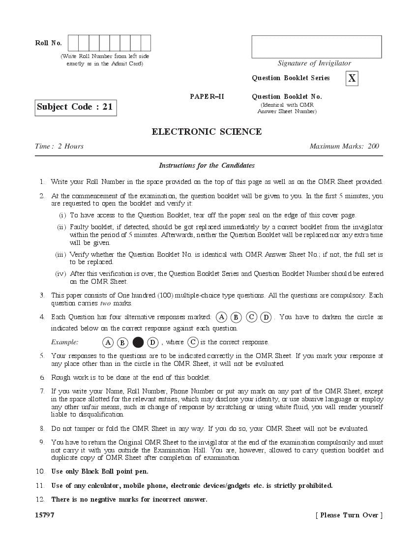
(Write Roll Number from left side
exactly as in the Admit Card) Signature of Invigilator
Question Booklet Series X
PAPER–II Question Booklet No.
Subject Code : 21 (Identical with OMR
Answer Sheet Number)
ELECTRONIC SCIENCE
Time : 2 Hours Maximum Marks: 200
Instructions for the Candidates
1. Write your Roll Number in the space provided on the top of this page as well as on the OMR Sheet provided.
2. At the commencement of the examination, the question booklet will be given to you. In the first 5 minutes, you
are requested to open the booklet and verify it:
(i) To have access to the Question Booklet, tear off the paper seal on the edge of this cover page.
(ii) Faulty booklet, if detected, should be got replaced immediately by a correct booklet from the invigilator
within the period of 5 minutes. Afterwards, neither the Question Booklet will be replaced nor any extra time
will be given.
(iii) Verify whether the Question Booklet No. is identical with OMR Answer Sheet No.; if not, the full set is
to be replaced.
(iv) After this verification is over, the Question Booklet Series and Question Booklet Number should be entered
on the OMR Sheet.
3. This paper consists of One hundred (100) multiple-choice type questions. All the questions are compulsory. Each
question carries two marks.
4. Each Question has four alternative responses marked: A B C D . You have to darken the circle as
indicated below on the correct response against each question.
Example: A B C D , where C is the correct response.
5. Your responses to the questions are to be indicated correctly in the OMR Sheet. If you mark your response at
any place other than in the circle in the OMR Sheet, it will not be evaluated.
6. Rough work is to be done at the end of this booklet.
7. If you write your Name, Roll Number, Phone Number or put any mark on any part of the OMR Sheet, except
in the space allotted for the relevant entries, which may disclose your identity, or use abusive language or employ
any other unfair means, such as change of response by scratching or using white fluid, you will render yourself
liable to disqualification.
8. Do not tamper or fold the OMR Sheet in any way. If you do so, your OMR Sheet will not be evaluated.
9. You have to return the Original OMR Sheet to the invigilator at the end of the examination compulsorily and must
not carry it with you outside the Examination Hall. You are, however, allowed to carry question booklet and
duplicate copy of OMR Sheet after completion of examination.
10. Use only Black Ball point pen.
11. Use of any calculator, mobile phone, electronic devices/gadgets etc. is strictly prohibited.
12. There is no negative marks for incorrect answer.
15797 [ Please Turn Over ]
Page 3
ELECTRONIC SCIENCE
PAPER II
1. In an intrinsic semiconductor the free electron 6. The diodes in the following circuit are ideal and
concentration depends on the input voltage ranges from –10V to +10V. The correct
(A) effective mass of electrons only. transfer characteristics of the following circuit is
(B) effective mass of holes only. D1 D2
(C) temperature of the semiconductor. +
1k
(D) width of the forbidden energy band of the V in
semiconductor. Vo
– D4
D3
2. The static characteristics of an adequately forward
biased p-n junction is a straight line, if the plot is of
(A) log I vs. log V Vo
(B) log I vs. V
10V
(C) I vs. log V
(D) I vs. V
–10V 0
(A) Vin
0 +10V
3. The diffusion potential across a p-n junction
(A) decreases with increasing doping
–10V
concentration.
(B) increases with decreasing band gap.
(C) does not depend on doping concentrations. Vo
(D) increases with increase in doping
10V
concentration.
4. The early-effect in a bipolar junction transistor is (B) 0 Vin
caused by –10V 0
(A) fast turn-on.
–10V
(B) fast turn-off.
(C) large collector-base reverse bias.
(D) large emitter-base forward bias.
Vo
5. In the following circuit, the values of V01 and V02 10V
in volts are + 6V
O
0 10V
1k (C) Vin
–10V
O V01
D1 D2 –10V
O V02
2k
Vo
O – 6V
(A) V01 = 6V, V02 = – 6V
(D) 0
(B) V01 = 2V, V02 = 8V Vin
–10V 0 +10V
(C) V01 = 2V, V02 = – 2V
(D) V01 = 4V, V02 = 2V
Page 4
7. A p-type semiconductor has been highly 11. The oxidation rate for wet oxidation system is
doped by trivalent impurity so as to make it degenerate. written as
The Fermi level of this semiconductor lies
dx 1
(A)
(A) at the middle of the forbidden energy gap. dt A 2 B ( x x0 )
(B) somewhere in the middle of the forbidden
dx
energy gap and the top of the valence band. (B) A B ( x x0 )
dt
(C) somewhere in the middle of the forbidden
energy gap and the bottom of the conduction dx
(C) A 2 B ( x x0 )
band. dt
(D) inside the valence band. dx 1
(D)
dt A B ( x x0 )
where A and B are constant, x = oxide thickness
and x0 = initial oxidation thickness.
8. The holes in a semiconductor are
(A) particles like electrons with opposite charge.
(B) particles with a mass equal to the free electron
mass at all positions of the energy bands. 12. The cut-off frequency of the following T-section
filter in kHz is
(C) vacancies in an otherwise filled valence band.
4F 4F
(D) quasi-particles which can exist inside both
the valence band and the conduction band.
5mH
9. Which of the following statements is not correct? 1
(A)
(A) A varactor diode can be used as a voltage
variable capacitor.
5
(B) The depletion layer width of a p-n junction is (B)
2
voltage dependent.
(C)
(C) The junction capacitance of a p-n junction
does not depend upon the bias voltage applied
to the junction. (D)
2
(D) The dynamic resistance of a forward biased
p-n junction is current-dependent.
13. The inverse Fourier transform of the function
1
F ( w) ( w) is
10. Metal deposition thickness does not depend on jw
(A) Impingement rate (A) sin wt
(B) Mass of metal (B) cos wt
(C) Density of metal (C) sin(t)
(D) Work function of metal (D) u(t)
Page 5
t
14. The Laplace transform of e sin(t) 17. Thevenin equivalent resistance R TH of the
following circuit is
a 6
(A)
a2 S 1
2 O
a 2A 6
(B)
a2 S 1
2
R TH
S 1 5V
(C)
a2 S 1
2
O
S 1 (A) 3
(D)
a S 1
2 2
(B) 12
(C) 6
(D) Infinity
15. If X (n) is a real sequence, then what is the value
of Xi (w)
(A) X (n)sin(wn) 18. h21 of the following network is
n
I1 R R
I2
(B) X ( n)sin(wn) +
O O
+
n
R
X (n)cos (wn)
V1 V2
(C)
n
– –
O O
(D) X ( n)cos(wn) 3
n (A)
2
1
(B)
2
16. In the network of figure shown below, the 1
maximum power is delivered to RL if its value is (C)
2
I1 3
(D)
2
20 RL 40
0.5 I1
50V
19. For a 2 port symmetrical bilateral network, if
transmission parameters A = 3 and B = 1, the value of
(A) 16 parameter C is
(A) 3
40
(B) (B) 8 S
3
(C) 8
(C) 60
(D) 9
(D) 20
Page 6
20. An amplifier has a open-loop gain 23. For the following transistor, = 99. The value of
Ao = 1000 100. Apply feedback to design an amplifier the output voltage, Vo, in the following circuit is
whose voltage gain varies no more than 0·1%. The gain +12·7V
with feedback is O
(A) 10 3k
(B) 100
(C) 200
O V
(D) 500 0
100k
0·7V
21. The output voltage (Vo) of the following circuit in
millivolt is (A) 3 V
3L
(B) 1 V
3 Sint (mv) L (C) 3·7 V
O
– (D) 0·7 V
O V
+ 0
O
Sint (mv) 2L
24. MOSFET devices the n-channel type is better
(A) – 3·5 sint than the p-channel type in the following respects:
(B) – 12 sint (A) It has better noise immunity.
(C) – 7 sint (B) It is faster.
(D) – 10·5 sint (C) It is TTL compatible.
(D) It has better drive capability.
22. The gain-bandwidth product of the following 25. One of the following is not the characteristics of
Op-Amp is 1 MHz. The bandwidth of this amplifier is a FET:
(A) Less temperature sensative
+ OV
(B) Low noise
– 0
(C) Voltage gain is high when used as an amplifier
+
V in (D) Unipolar device
– 9k
1k
26. The ‘pinch-off’ voltage of a JFET is 5·0 volts, its
‘cut-off’ voltage is
1
(A) 1 MHz (A) 5·0 2 V
(B) 100 kHz (B) 2·5 V
(C) 10 kHz (C) 5·0 V
3
(D) 5·0 2 V
(D) 10 MHz
Page 7
27. In a transistor push-pull amplifier 32. If the Op-Amp in the figure has an input offset
voltage of 5mV and an open loop voltage gain of 10,000;
(A) there is no dc present in the output.
then V0 will be
(B) there is no distortion in the output. +15V
(C) there is all even harmonics in the output.
–
(D) there is no odd harmonics in the output.
V0
+
28. Negative feedback in amplifiers
–15V
(A) improves the signal to noise ratio at the input.
(B) improves the signal to noise ratio at the
(A) 0 V
output.
(B) 5 mV
(C) does not effect the signal to noise ratio at the
output. (C) + 15V to –15 V
(D) reduces distortion. (D) + 50V to – 50 V
29. FET is very popular as
(A) high gain amplifier.
(B) low noise amplifier.
(C) large gain bandwidth product type amplifier.
(D) low input impedance amplifier.
30. Two identical FETs, each characterized by the
parameters gm and rd are connected in parallel. The 33. The combinational circuit implemented using PLA
composite FET is then characterized by the parameters. shown in the figure is
gm
(A) and rd A
2
gm r B
(B) and d
2 2
rd C
(C) 2gm and
2
(D) 2gm and 2rd
F1
F2
31. The Eber–Moll model is applicable to
(A) Bipolar Junction Transistor (A) Half Adder
(B) NMOS Structure (B) Half Subtractor
(C) Unipolar Junction Transistors (C) Full Adder
(D) Junction Field Effect Transistor (D) Full Subtractor
Page 8
34. The simplified POS expression for the following 37. The simplification of the Boolean function
Boolean function: – – – –
F = AB C + B + BD + ABD +AC will be
F (A, B, C, D) = m (0, 1, 4, 6, 8, 14, 15) d (2, 3, 9)
(A) B
is –
– – – (B) A + B
(A) (A + D) (B + C + D) (A + B + C )
(C) C + A
(B) (ACD + B) (A + B + C)
– – (D) B + C
(C) (A + B + C) (A + B ) (A + C)
– – –
(D) (B + C) (A + D) (A + B + C )
38. An asynchronous counter is shown in the figure.
The mode number of the counter is
1
J0 Q0 J1 Q1 J2 Q2 J3 Q3 J4 Q4
35. The NAND TTL 74LS00 has the following
K0 Q0 K 1 Q1 K2 Q2 K 3 Q3 K4 Q4
current ratings:
IOLmax = 15 mA, IILmax = –0·6 mA, IOHmax = –450 A, and
IIHmax = 30 A. (A) 24
The fan out of the gate will be (B) 28
(A) 15 (C) 29
(B) 25 (D) 48
(C) 40
(D) 50 39. For the function Y to be 1 in the combinational
circuit shown in the figure, the input combination is
A
B Y
36. The Boolean function implemented in the
following multiplexer circuit is C
1 I0 (A) A = 1, B = 1, C = 0
A . . I1
0. I2
(B) A = 1, B = 0, C = 0
1. I3
Y
(C) A = 0, B = 1, C = 0
I4 (D) A = 0, B = 0, C = 1
0. I5
1. I6
I7
40. It is required to count a pulse train having a
S2 S1 S0
frequency of 1 MHz using a modulo 1024 ripple counter.
B C D The maximum permissible propagation delay is
(A) m (0, 1, 3, 4, 6, 7) (A) 1 s
(B) m (1, 4, 9, 13, 15) (B) 10 s
(C) m (0, 1, 3, 6, 7, 8, 11, 12, 14) (C) 10 ns
(D) m (2, 3, 5, 6, 10, 11, 13, 14) (D) 100 ns
Page 9
41. The Boolean function ‘Y’ implemented in the 43. Conversion time of a certain A/D converter of the
folowing circuit is successive approximation type for digitizing an analogue
VDD = –15 V signal that is 1/4th full scale value is 2·5s. the conversion
time for this converter for digitizing an analogue signal
that is half of full scale value would be
Y (A) 5 s
A B C (B) 10 s
(C) 1·25 s
D (D) 2·5 s
(A) (A + B + C) D
(B) ABC + D 44. In an antifuse FPGA, logic cell must consider
(A) more inputs (more than 4 inputs).
(C) A + B + CD
(B) more outputs (more than 4 outputs).
(D) C + D AB (C) less inputs and outputs (less than and equal
to 4).
(D) more outputs and more inputs.
42. library ieee;
use ieee: std_logic_1164 all;
entity add4 is port ( 45. A binary multiplier is designed to multiply two
5 bit binary numbers. Size of ROM would be
a, b : in std_logic_vector (3 down to 0)
C1 : in std_logic (A) 64 × 4
sum : out std_logic_vector (3 down to 0) (B) 1024 × 6
C0 : out std_logic); (C) 64 × 8
end add4;
(D) 128 × 6
The symbolic equivalent circuit is shown in which
figure?
C1
46. Which of the following signal is used when
a (3:0) sum (3,0)
microprocessor wants to address the memory?
(A)
1
b (3:0) C0 (3:0) (A) Io/M
(B) Status signal
C1
(C) ALE
a (3:0) sum (3:0)
(B) (D) HOLD and HLDA
b (3:0) C0
a (3:0) sum (3:0)
(C) 47. Microprocessors are programmed using
b (3:0) C0 (3:0) (A) Assembly language
(B) Pascal
a (3:0) b (3:0)
(C) High level language such as C, C++
(D)
sum (3:0) C0 (D) Fortran
Page 10
48. A set of 8085 instructions is given below: 52. A microcontroller is to be programmed to generate
MVI A, A9H a square waveform with minimum and maximum time
MVI B, 57H periods of 100 nS and 10 mS. What is clock frequency
ADD B required for the above?
ORA A (A) 100 Hz
The flag status (S, Z, Cy) after the instruction (B) 1 MHz
ORA A is executed as (C) 10 MHz
(A) (0, 1, 1) (D) 0·1 MHz
(B) (1, 0, 0)
(C) (0, 1, 0)
(D) (1, 0, 1)
53. Find the resistance where I = 20 mA, Vcc = 5V
VLED = voltage across LED = 1·5V.
49. Consider the following loop: Vcc Vcc
LXI B, 000AH
LOOP : DCX B
LED
MOV A, B
ORA C Microcontroller
JNZ LOOP I
The loop is executed by
(A) 1 time
(B) 10 times GND
(C) 11 times (A) 175 Ohm
(D) Infinite times (B) 1750 Ohm
(C) 17·5 Ohm
50. The contents of the accumulator after the (D) 1780 Ohm
execution of following instruction will be
MVI A, A 7H
ORA A 54. A 64k RAM chip can store
RLC (A) 64000 bytes
(A) C F H (B) 65536 bytes
(B) 4 F H (C) 65536 bits
(C) 4 E H (D) 64000 bits
(D) C E H
51. An 8k × 8 bit RAM is interfaced to an 8085 55. An n-type GaAs Gunn diode operates in the
microprocessor. In the decoded scheme if the address of transit time mode with a frequency of oscillation equal to
the last memory location of this RAM is 4FFFH, the 10 GHz. The drift velocity of electrons is 2·5×107 cm/sec.
address of the first memory location of the RAM will be The length of the device in m is
(A) 1000A (A) 2·5
(B) 2000H (B) 50
(C) 3000H (C) 12·5
(D) 4000H (D) 25
Page 11
56. The attenuation constant of a network, = 1 neper. 60. An end-fire array of 8 half-wave dipole elements
The value of in dB will be produces the principal lobe along the line of the array.
The signal frequency is 1·5 GHz and the antenna elements
(A) 0 are uniformly spaced with an inter-element spacing
(B) 2·302 of 4. The width of the principal lobe of this array in
(C) 0·434 radian is
(D) 8·686 (A) 1
(B) 0·5
57. The phase velocity of a 2 kHz signal propagating (C) 2
on a distortionless transmission line having L and C as
(D) 0·75
loop inductance and capacitance per unit length of the
line respectively, can be expressed as
1
(A)
LC
61. A hollow metallic waveguide with its rectangular
1 cross-section of 2 cm × 1 cm has its cut-off wavelength
(B) in cm for the TE10 mode equal to
2LC
(A) 4
(C) LC
(B) 1
L (C) 2
(D)
C (D) 0·5
58. [Sij] is the scattering matrix of a lossless microwave
circulator where i, j = 1, 2, 3. The wave flows from ports
1 2 3 in the clockwise direction. Sij is the scattering
62. A hollow, metallic waveguide with rectangular
matrix element for the wave incident at part ‘j’ and
cross-section of 4 cm × 3 cm. The ratio of cut-off
emerging from port ‘i’. The value of S13 will be
frequencies for TE10 and TM11 modes is
(A) 1
(A) 1 : 8
(B) 0 (B) 2 : 5
1 (C) 3 : 4
(C)
2 (D) 3 : 5
1
(D)
2
59. Maxwell’s fundamental contribution in the 63. A two-cavity klystron amplifier using identical
formulation of electromagnetic field equations was in buncher and catcher cavities and operating at 5GHz has
the equation the following parameter values.
(A) . B 0 DC accelerating voltage, Vdc = 200 V cavity gap
width, d = 1mm
(B) . D The value of the beam coupling coefficient of the
buncher cavity is
(C) E B
t (A) 0·921
D J (B) 0·357
(D) H
t (C) 0·509
(The symbols have their usual significances.) (D) 0·715
Page 12
64. A TWT amplifier is designed to amplify 8 GHz 68. Blind speed of a radar —
microwave signal and it operates with a dc accelerating
(A) Radar rotates at such a high speed it cannot
voltage of 1000 volts. The dc electron beam current is
see anything.
15mA. The helix has a length of 7 cm and a characteristic
impedance of 20 . The power gain of the TWT in dB is (B) The target is moving at such a high speed
that phase differences between successive
(A) 49·92 pulses will be zero.
(B) 29·86 (C) Target is at such a distance radar cannot see
(C) 53·15 it.
(D) 59·46 (D) All the above statements are correct.
69. Side lobe of an antenna pattern causes
(A) reduced bandwidth.
65. A cylindrical magnetron having a cathode radius (B) reduced antenna gain.
of 6 cm and anode radius of 12 cm measured from the (C) ambiguity in direction finding.
centre of the cathode is operated with a crossed magnetic
field with magnetic flux density of 2 mWeber/m2. The (D) increased antenna gain.
cut-off anode voltage of this magnetron in volt is
(A) 564 70. The type of radar that is used to eliminate clutter
(B) 900 in navigational application is
(C) 712 (A) MTI radar
(D) 1200 (B) Pulse radar
(C) Monopulse radar
(D) Tracking radar
66. You are asked to increase the maximum range of
the pulsed radar by increasing the transmitter Peak Power 71. If ‘fc’ be cut-off frequency of the waveguide and
only. To double the existing maximum range of this ‘f’ be the operating frequency then
radar, the transmitter Peak Power has to be increased by (A) f = fc
a factor of
(B) f < fc
(A) 4
(C) f > fc
(B) 8
(C) 32 (D) f << fc
(D) 16
72. The degenerated modes in a waveguide are
characterized by
(A) same cut-off frequencies and same field
67. An MTI radar operates at 3 GHz with a pulse distributions.
repetition frequency of 1 kHz. The first blind speed of this (B) same cut-off frequencies and different field
radar in km/hour is distributions.
(A) 120 (C) different cut-off frequencies but same field
(B) 180 distributions.
(C) 360 (D) different cut-off frequencies and different
(D) 720 field distributions.
Page 13
73. The wavelength of electromagnetic waves in a 78. The magnitudes of the open-circuit and
waveguide short-circuit input impedances of a transmission line are
100 and 25 respectively. The characteristic
(A) is inversely proportional to the phase velocity.
impedance of the line is
(B) is greater than that in free space. (A) 25
(C) is directly proportional to the phase velocity. (B) 50
(D) depends only on the waveguide dimensions (C) 75
and free space wavelength. (D) 100
74. Condition for minimum attenuation is
(A) RG = LC 79. To overcome difficulties with strapping high
frequencies, the type of cavity structure desired for
(B) RC = LG magnetron is
(C) GC = LR (A) hole and slot
(B) slot
(D) RL = GC
(C) vane
(D) rising sun
75. The magnetic field at a distance r from the center
of the wire is proportional to
(A) r for r < a and 1 r2 for r > a 80. The following diode does not use negative
resistance in its operation:
(B) 0 for r < a and 1 r for r > a (A) Gunn diode
(B) Tunnel diode
(C) r for r < a and 1 r for r > a (C) Backward diode
(D) IMPATT diode
(D) 0 for r < a and 1 r2 for r > a
81. The major advantage of TWT over a klystron lies
76. Vector potential is a vector in the
(A) whose curl is equal to the magnetic flux (A) higher bandwidth
density.
(B) higher gain
(B) whose curl is equal to the electric field
(C) higher frequency
intensity.
(D) higher output power
(C) whose divergence is equal to the electric
potential.
(D) which is equal to the vector product E × H.
82. A 10kW carrier is sinusoidally modulated by
two modulating signals corresponding to a modulation
77. For an ideal waveguide if reflection coefficient index of 30% and 40% respectively. The total radiated
= 1, then the correspoinding value of VSWR is power is
(A) 0 (A) 11·25 kW
(B) 1 (B) 12·5 kW
(C) ½ (C) 15 kW
(D) (D) 17 kW
Page 14
83. The Fourier transform of a conjugate symmetric 88. A system has three stage cascaded amplifier, each
function is always stage having a power gain of 20dB and noise figure of
(A) Real 6dB. The overall noise figure is
(B) Imaginary (A) 1·38
(C) Conjugate anti-symmetric (B) 6·8
(D) Conjugate symmetric (C) 4·33
(D) 10·43
84. The orbital motion of a satellite is governed by 89. Three analog signals, having bandwidths 1200 Hz,
(A) Maxwell’s equations 600 Hz and 600 Hz, are sampled at their respective
(B) Euler equations nyquist rates, encoded with 12 bit words, and time
division multiplexed. The bit rate for the multiplexed
(C) Kepler’s laws
signal is
(D) Newton’s laws
(A) 57·6 kbps
(B) 115·2 kbps
(C) 28·8 kbps
(D) 38·4 kbps
85. The probabilities of transmitted symbols from a
zero-memory source are given by p1=0·5, p2=0·25,
p3= p4= 0·125. The entropy of the source is
(A) 2 bit 90. In a PCM system, the number of quantization
(B) 1 bit levels is 16 and the maximum signal frequency is 4 kHz;
the bit transmission rate is
(C) 0·75 bit
(A) 32 bits/s
(D) 1·75 bit
(B) 16 bits/s
(C) 64 kbits/s
(D) 32 kbits/s
86. The attenuation of the optical fiber used in an
optical fiber link is 0·8 dB/km. When an optical power of
150 mw is connected at the input, the output power 91. An optical power of 120 w is launched into a
results 10 mw. The maximum optical fiber length of the single input port of a 16 × 16 fused fiber star coupler.
link is The power measured at the output port is 10 w. The
(A) 12·7 km splitting loss of the coupler is
(B) 14·7 km (A) 0·97 dB
(C) 20·5 km (B) 10·8 dB
(D) 25·7 km (C) 12·04 dB
(D) 0·77 dB
87. The bulk carrier recombination life time for a 92. A silicon PIN photodetector has a junction
GaAlAs LED is 25 nS and the LED emits an optical capacitance of 18pF, active area of 12 mm2 and a
power of 250 w at constant DC current. The optical responsivity of 0·6 A/W. When it is illuminated with an
power output of the LED when modulate data frequency optical power of 0·5 mw /cm2, the voltage obtained
of 120 MHz is across a load resistance of 120 k would be
(A) 13·24 w (A) 5·8 V
(B) 16·27 w (B) 6·8 V
(C) 35·82 w (C) 4·3 V
(D) 40·52 w (D) 2·7 V
Page 15
93. A resistance strain gauge has a gauge factor of 2·8 97. An accelerometer has a scismic mass of 0·05kg
and it is fastened to a steel member subjected to a stress and spring constant of 3×10³ N/m. If maximum
of 120 N/mm2. The modulus of elasticity of steel is displacement of mass is 1 mm, the maximum
2·5 × 105 N/mm2. The percentage change in resistance is acceleration which can be measured is
(A) 1·12 (A) 120 m/Sec2
(B) 0·02 (B) 90 m/Sec2
(C) 0·336 (C) 60 m/Sec2
(D) 0·134 (D) 30 m/Sec2
94. Two wattmeters are connected to a three phase
system supplying a balanced load and the readings are 98. Potentiometer sensitivity can be increased by
10·5 kW and 2·5 kW respectively. The total power and
(A) decreasing the current in potentiometer wire.
power factor are
(B) increasing the length of potentiometer wire.
(A) 8·0 kW and 0·52
(C) decreasing the length of potentiometer wire.
(B) 8·0 kW and 0·335
(D) replacing the standard cell by a regulated
(C) 13·0 kW and 0·334
power supply.
(D) 13·0 kW and 0·684
95. A signal 12 coswt + 6 cos2wt is applied on a
spectrum analyzer. In the analyzer, it will be seen as 99. The TRIAC can be used only in
(A) a single waveform like a rectangular pulse. (A) inverter
(B) two waveform of w and 2w. (B) rectifier
(C) a spike of 18 volts at w and 2w. (C) multi-quadrant chopper
(D) two spikes of 12 volts at w and 6 volts at 2w. (D) cycloconverter
96. An oscilloscope has 50 mV/ divn. and a square
pulse is applied to its vertical plate. In the output, the 100. The entries in the first column of Routh array of a
leading edge has 3·5 divisions and trailing edge 3 divisions. fourth order are 5, 2, – 0·1, 2, 1. The number of poles in
The tilt is the right half plane are
(A) 13·9 % (A) 1
(B) 15·4 % (B) 2
(C) 16·6 % (C) 3
(D) 20·5 % (D) 4
Page 16
ROUGH WORK
Page 17
ROUGH WORK
Page 18
ROUGH WORK
Page 19
ROUGH WORK
Page 20
ROUGH WORK
Document Details
| Board / Org | Default |
| Exam | Govt Jobs Exams |
| Type | Question Paper |
| Pages | 20 |
| Updated | 30 Apr 2026 |