CUSAT CAT 2023 Question Paper Electronics
Finished viewing? Save it for later —
Download CUSAT CAT 2023 Question Paper Electronics (PDF · 29 pages)About CUSAT CAT 2023 Question Paper Electronics
CUSAT CAT 2023 Question Paper Electronics is available here for free download. Published by Cochin University for CUSAT Common Admission Test, this question paper can be viewed online or downloaded as a PDF (29 pages). Candidates preparing for CUSAT Common Admission Test can use CUSAT CAT 2023 Question Paper Electronics to understand the exam pattern, the type of questions asked, and the overall difficulty level.
Frequently Asked Questions
How can I download CUSAT CAT 2023 Question Paper Electronics?
Open this page and click the Download button to save CUSAT CAT 2023 Question Paper Electronics as a PDF. It is completely free on AglaSem Docs.
Is CUSAT CAT 2023 Question Paper Electronics free to download?
Yes. CUSAT CAT 2023 Question Paper Electronics can be viewed online and downloaded as a PDF free of cost on AglaSem Docs.
How many pages does CUSAT CAT 2023 Question Paper Electronics have?
CUSAT CAT 2023 Question Paper Electronics contains 29 pages, which you can read online or download together as a single PDF.
Where can I find more CUSAT Common Admission Test study material?
You can find more CUSAT Common Admission Test question papers, sample papers, syllabus, and answer keys on AglaSem Docs.
CUSAT CAT 2023 Question Paper Electronics – Text
Read the full text of this question paper below — useful to quickly search, copy and reference the content online without downloading the PDF.
📄 View text version (29 pages)
Page 1
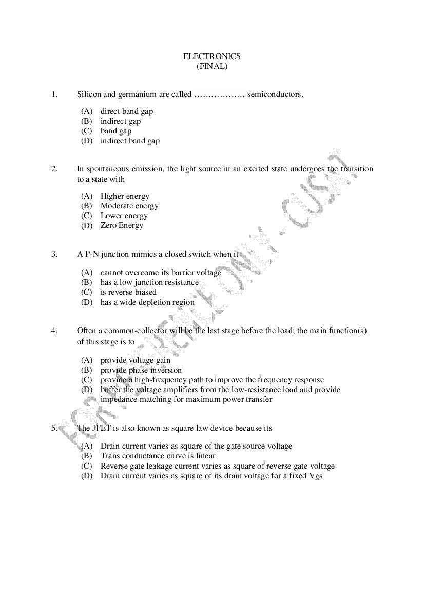
(FINAL)
1. Silicon and germanium are called ……………… semiconductors.
(A) direct band gap
(B) indirect gap
(C) band gap
(D) indirect band gap
2. In spontaneous emission, the light source in an excited state undergoes the transition
to a state with
(A) Higher energy
(B) Moderate energy
(C) Lower energy
(D) Zero Energy
3. A P-N junction mimics a closed switch when it
(A) cannot overcome its barrier voltage
(B) has a low junction resistance
(C) is reverse biased
(D) has a wide depletion region
4. Often a common-collector will be the last stage before the load; the main function(s)
of this stage is to
(A) provide voltage gain
(B) provide phase inversion
(C) provide a high-frequency path to improve the frequency response
(D) buffer the voltage amplifiers from the low-resistance load and provide
impedance matching for maximum power transfer
5. The JFET is also known as square law device because its
(A) Drain current varies as square of the gate source voltage
(B) Trans conductance curve is linear
(C) Reverse gate leakage current varies as square of reverse gate voltage
(D) Drain current varies as square of its drain voltage for a fixed Vgs
Page 2
(i) The gate circuit impedance of MOSFET is higher than that of a BJT
(ii) The gate circuit impedance of MOSFET is lower than that of a BJT
(iii) The MOSFET has higher switching losses than that of a BJT
(iv) The MOSFET has lower switching losses than that of a BJT
(A) Both (i) and (ii)
(B) Both (ii) and (iv)
(C) Both (i) and (iv)
(D) Only (ii)
7. Which of the following is most difficult to fabricate in an IC?
(A) Diode
(B) Transistor
(C) FET
(D) Capacitor
8. In FET the drain voltage above which there is no increase in the drain current is called
(A) Critical Voltage
(B) Pinch off Voltage
(C) Breakdown Voltage
(D) Cut off Voltage
9. Which of the following is true about a PIN diode?
(A) Its photosensitive in reverse bias
(B) It offers low resistance and low capacitance
(C) It has a decreased reversed breakdown voltage
(D) Carrier storage is low
10. Superposition theorem states that the response in any element is the ……………… of
the responses that can be expected to flow if each source acts independently of other
sources.
(A) sum
(B) algebraic sum
(C) product
(D) subtraction
Page 3
Determine 50 voltage
source
(A) 6.42 ∠ 77.47°
(B) 6.42 ∠ −77.47°
(C) 5.42 ∠ 77.47°
(D) 5.42 ∠ −77.47°
12. nin resistance across the terminal
Calculate the Thevenin terminal AB for the following circuit
(A) 4.34 ohm
(B) 3.67 ohm
(C) 3.43 ohm
(D) 2.32 ohm
13. The equivalent value of the 3 resistances when connected in star connection is
(A) 2.32 ohm, 1.22 ohm, 4.54 ohm
(B) 3.55 ohm, 4.33 ohm, 5.67 ohm
(C) 2.78 ohm, 1.67 ohm, 0.83 ohm
(D) 4.53 ohm, 6.66 ohm, 1.23 ohm
Page 4
(A) Electrolyte capacitor
(B) Mica capacitor
(C) Air capacitor
(D) Glass capacitor
15. Mesh analysis is generally used to determine
(A) Voltage
(B) Current
(C) Resistance
(D) Power
16. If the resonant peak is estimated to be '5', which among the following would be the
correct value of damping?
(A) ξ = 0.3
(B) ξ=1
(C) ξ = 3.2
(D) ξ = 5.55
17. Which of the following circuit has unity Power factor?
(A) Inductive circuit
(B) Capacitive circuit
(C) Resistive circuit
(D) Conductive circuit
18. The rms value of the voltage for a voltage function v = 10 + 5 cos(628t + 300)v
through a circuit is
(A) 5V
(B) 10 V
(C) 10.6 V
(D) 15 V
19. Which logic is the fastest of all the logic families?
(A) TTL
(B) ECL
(C) HTL
(D) DTL
Page 5
(A) high noise immunity
(B) low static power consumption
(C) high resistivity
(D) both high noise immunity and low static power consumption
21. In a 3-input XNOR gate, how many of input possibilities will result in a HIGH
output?
(A) 1
(B) 7
(C) 4
(D) 6
22. Knowledge of propagation delay is important because
(A) the logic gates must be given a short break during each clock cycle or else they
will overheat
(B) it limits the maximum operating frequency of a gate
(C) it is a measure of how long the clock must be applied to the gate before it will
make the required decision
(D) all the gates in a system must have the same propagation times in order to be
compatible
23. Which statement below best describes a Karnaugh map?
(A) A Karnaugh map can be used to replace Boolean rules
(B) The Karnaugh map eliminates the need for using NAND and NOR gates
(C) Variable complements can be eliminated by using Karnaugh maps.
(D) Karnaugh maps provide a visual approach to simplifying Boolean expressions.
24. Sample-and-hold circuits in ADCs are designed to
(A) sample and hold the output of the binary counter during the conversion process
(B) stabilize the ADCs threshold voltage during the conversion process
(C) stabilize the input analog signal during the conversion process
(D) sample and hold the ADC staircase waveform during the conversion process
Page 6
Group I Group II
(P) Multiplexer (1) increment/decrement
(Q) Decoder (2) one to many
(R) Demultiplexer (3) one output
(S) Counter (4) many to one
(A) (P)-(3), (Q)-(1), (R)-(4), (S)-(2)
(B) (P)-(2), (Q)-(3), (R)-(4), (S)-(1)
(C) (P)-(2), (Q)-(3), (R)-(1), (S)-(4)
(D) (P)-(3), (Q)-(1), (R)-(2), (S)-(4)
26. In a flash analog-to-digital converter, the output of each comparator is connected to an
input of a
(A) decoder
(B) priority encoder
(C) multiplexer
(D) demultiplexer
27. The number of software interrupts in 8085 is
(A) 5
(B) 8
(C) 9
(D) 10
28. Which of following is both level and edge sensitive?
(A) RST 7.5
(B) RST 5.5
(C) TRAP
(D) INTR
29. The Program Counter in a microprocessor
(A) Counts the number of instructions executed in a program
(B) Counts the number of programs run by the processor
(C) Points to the next executable instruction
(D) Points to the present or next executable instruction
Page 7
(A) 34 K
(B) 44K
(C) 54 K
(D) 64 K
31. In an 8085 based system, the maximum number of input output devices can be
connected using I/O mapped I/O method is
(A) 64
(B) 512
(C) 256
(D) 65536
32. In order to complement the lower order nibble of the accumulator, we can use
(A) ANI 0FH
(B) XRI 0FH
(C) ORI 0FH
(D) CMA
33. The contents of registers A and B after execution of following instructions are
XRA A
MVI B, 4AH
SUI 4FH
ANA B
HLT
(A) 05,4A
(B) 4F, 00
(C) B1, 4A
(D) 00,4A
34. BHE of 8086 microprocessor signal is used to interface the
(A) Even bank memory
(B) Odd bank memory
(C) I/O
(D) DMA
Page 8
(A) I/O can be interfaced in MAX / MIN mode
(B) Supports pipelining
(C) Coprocessor is interfaced in MIN mode
(D) Coprocessor is interfaced in MAX mode
36. ……………… memory locations can be addressed directly by Intel 8086
(A) 64K
(B) 512K
(C) 1M
(D) 1K
37. Which of the following is NOT TRUE with respect to 8086 microprocessor
(A) Physical address of the memory is generated by bus interface unit
(B) Instruction queue is used to store data to be processed by next instruction
(C) It contains only 4 segment registers
(D) It supports multiplication and division operation
38. JFET can operate in
(A) depletion mode only
(B) enhancement mode only
(C) either depletion or enhancement modes at a time
(D) both depletion and enhancement modes simultaneously
39. A half-wave rectifier circuit with a capacitive filter is connected to a 200 volts, 50 Hz
ac line. The output voltage across the capacitor should be approximately
(A) 300 V
(B) 280 V
(C) 180 V
(D) 80 V
40. For single phase supply frequency of 50 Hz, ripple frequency in full wave rectifier is
(A) 25
(B) 50
(C) 100
(D) 200
Page 9
(A) Phase control
(B) Integral control
(C) Chopper
(D) Inverter
42. ……………… is used for critical loads where temporary power failure can cause a
great deal of inconvenience
(A) SMPS
(B) UPS
(C) MPS
(D) RCCB
43. Basic purpose of multistage arrangement is to increase the amplifiers overall
(A) Current gain
(B) Voltage gain
(C) Base resistance
(D) Slew rate
44. The relation between α and β is
α
(A) β=
(1 − α )
β
(B) α =
(1 + β )
α
(C) β =
(1 + α )
β
(D) α =
(1 − β )
45. What should be the value of input resistance for an ideal voltage amplifier circuit?
(A) Zero
(B) Unity
(C) Infinity
(D) Unpredictable
Page 10
(A) LC tank circuit
(B) Biasing circuit
(C) Transistor
(D) Power supply
47. In an LC circuit, when the capacitor is maximum, the inductor energy is
(A) Minimum
(B) Maximum
(C) Half-way between maximum and minimum
(D) Unpredictable
48. Multivibrators belong to a family of oscillators commonly called
(A) Relaxation oscillators
(B) Dynamic oscillators
(C) Stretched oscillators
(D) Static oscillators
49. The expression for short circuit current gain of an FET is given by
gm
(A)
ωC gs
Ig
(B)
g mVc
ωC gs
(C)
gm
Ig
(D)
gm Ic
50. The output of a particular Op-amp increases by 8 V in 12 µs. The slew rate is
(A) 90 V/µs
(B) 0.67 V/µs
(C) 1.5 V/µs
(D) 1.55 V/µs
Page 11
output voltage?
(A) Thevenin’s theorem
(B) Norton’s theorem
(C) Miller’s theorem
(D) Superposition theorem
52. In a super heterodyne receiver
(A) the IF stage has better selectivity than RF stage
(B) the RF stage has better selectivity than IF stage
(C) the RF stage has same selectivity than IF stage
(D) No selective capability in RF stage
53. In a broadcast superheterodyne receiver
(A) the local oscillator operates below the signal frequency
(B) local oscillator frequency is normally double the IF
(C) RF amplifier normally works at kHz above the carrier frequency
(D) mixer input must be tuned to the signal frequency
54. In a radio receiver with simple AGC
(A) the highest AGC voltage is produced between stations
(B) the faster the AGC time constant, the more accurate the output
(C) an increase in signal strength produces more AGC
(D) the audio stage gain is normally controlled by AGC
55. Fidelity of a receiver represents
(A) the sensitivity expressed in terms of voltage that must be applied to the receiver
input to give a standard output
(B) the extent to which the receiver is capable of distinguishing between the
desired signal and other frequencies
(C) the variation of the output with the modulation frequency when the output
impedance is a resistance
(D) the extent to which the receiver is not capable of distinguishing between the
desired signal and other frequencies
56. A transponder is a satellite equipment which
(A) receives a signal from Earth station and amplifies
(B) changes the frequency of the received signal
(C) retransmits the received signal
(D) does all of the above mentioned functions
Page 12
(A) 1
(B) 3
(C) 10
(D) 5
58. Which of the following is taken as reference antenna for directive gain?
(A) Half wave dipole
(B) Elementary doublet
(C) Isotropic
(D) Infinitesimal dipole
59. In phase shift keying the input signal is
(A) st(t) = A cos ω0t and s2(t) = −A cos ω0t
(B) s1(t) = s2(t) = A cos ω0t
(C) s1(t) = A cos ω0t and s2(t) = A cos (ω0t + p/2)
(D) s1(t) = A cos ω0t and s2(t) = −A (cos ω0t + p/2)
60. A 400 W carrier is amplitude modulated with m = 0.75. The total power in AM is
(A) 400 W
(B) 512 W
(C) 588 W
(D) 650 W
61. The klystron tube used in a klystron amplifier is a……………. type beam amplifier.
(A) Linear beam
(B) Crossed field
(C) Parallel field
(D) Crossed beam
Page 13
2Z L
(A)
( Z L + Z0 )
( Z L − Z0 )
(B)
( Z L + Z0 )
2Z0
(C)
( Z L + Z0 )
( Z L + Z0 )
(D)
( Z L − Z0 )
63. Which of the following statements are true about metals?
(A) Metals have a positive temperature coefficient
(B) Metals have a negative temperature coefficient
(C) Metals have zero temperature coefficient
(D) Metals have infinite temperature coefficient
64. Which among the following is an expression for energy?
2
(A) V It
2
(B) V Rt
V2t
(C)
R
V2t 2
(D)
R
65. Which among the following expressions relate charge, voltage and capacitance of a
capacitor?
(A) Q = C/V
(B) Q = V/C
(C) Q = CV
2
(D) C=Q V
Page 14
reached?
(A) 8V
(B) 0V
(C) 10 V
(D) Infinity
67. erromagnetic core is inserted into an inductor, what happens to the flux
When a ferromagnetic
linkage?
(A) Increases
(B) Decreases
(C) Remains the same
(D) Becomes zero
68. At resonance,
sonance, bandwidth includes the frequency range
ran that allows………………
………………
percent of the maximum current to flow.
(A) 33.33
(B) 66.67
(C) 50
(D) 70.7
69. If the resonant
esonant frequency in a series RLC circuit is 50 kHz along with a bandwidth of
5 kHz, find the quality factor.
(A) 5
(B) 50
(C) 10
(D) 500
70. Carrier
er swing is defined as
(A) The total variation in frequency from the lowest to the highest point
(B) Frequency deviation above or below the carrier frequency
(C) Width of the side band
(D) Amplitude of the side band
Page 15
small power.
(A) True
(B) False
(C) It depends on frequency
(D) It depends on modulation
72. What is the function of RF mixer?
(A) Addition of two signals
(B) Multiplication of two signals
(C) Subtraction of two signals
(D) To reduce the amount of noise
73. By which phenomenon does the energy transmission take place between the walls of
the tube in waveguides?
(A) Reflection
(B) Refraction
(C) Dispersion
(D) Absorption
74. The primary purpose of the helix in a traveling-wave tube is to
(A) prevent the electron beam from spreading in the long tube
(B) reduce the axial velocity of the RF field
(C) ensure broadband operation
(D) reduce the noise figure
75. A magic-Tee is nothing but
(A) a modification of F-plane tee
(B) a modification of H-plane tee
(C) a combination of E-plane and H-plane
(D) two E-plane tees connected in parallel
76. In matched line, the transmission coefficient is
(A) 0
(B) 1
(C) −1
(D) Infinity
Page 16
ability of
(A) Light Collection
(B) Light Scattering
(C) Light Dispersion
(D) Light Polarization
78. If all the transmission zeros of a network are at infinity then it is a
(A) High pass filter
(B) Low pass filter
(C) Band pass filter
(D) Band reject filter
79. In a balanced Wheatstone bridge, if position of defector and source are interchange
then bridge will still remain balanced. This inference can be drawn from
(A) Duality principle
(B) Reciprocity Principle
(C) Compensation theorem
(D) Equivalence theorem
80. Clamping circuits are one which
(A) inserts AC component in signal
(B) inserts DC component in signal
(C) insert both AC and DC
(D) filter AC component
81. An ideal constant voltage source has ……………… internal impedance whereas a
constant current source has ……………… internal impedance.
(A) infinite, zero
(B) zero, zero
(C) zero, infinite
(D) infinite, infinite
82. For a parallel resonant circuit with R = 2 Ω, L = 8 H, C = 2 F the quality factor is
(A) 0.5
(B) 1
1
(C)
2
(D) 2
Page 17
(A) very small as compared to speed of light
(B) varies with speed of light
(C) almost equal to speed of light
(D) greater than speed of light
84. When a number of different valued resistors are connected in series, the voltage drop
across each of the resistor is
(A) proportional to resistance
(B) inversely proportional to current
(C) proportional to square of current
(D) equal
85. Two wires A and B of same material and length l and 2l have radius r and 2r
respectively. The ratio of their specific resistance will be
(A) 1:4
(B) 1:2
(C) 1:1
(D) 1:8
86. An RC differentiator acts as a
(A) Low pass filter
(B) High pass filter
(C) Band pass filter
(D) Band stop filter
87. Laplace transform if sin(at )u (t ) is
s
(A)
a + s2
2
a
(B)
a + s2
2
s2
(C)
a2 + s2
a2
(D)
a2 + s2
Page 18
(A) linear operation
(B) non linear operation
(C) static operation
(D) dynamic operation
89. Laplace transform for continuous time signals is a
(A) time domain approach
(B) frequency domain approach
(C) distance domain approach
(D) coordinated domain approach
90. The network function N(S) becomes ……………… when s is equal to anyone of the
zeros.
(A) 1
(B) 2
(C) 0
(D) ∞
91. If the poles or zeros are not repeated, then the function is said to be having
……………… poles or ……………… zeros
(A) simple, multiple
(B) multiple, simple
(C) simple, simple
(D) multiple, multiple
92. The expression of ωr in parallel resonant circuit is
1
(A)
2 LC
1
(B)
LC
1
(C)
π LC
1
(D)
2π LC
Page 19
(A) ground
(B) trigger
(C) output
(D) reset
94. Under which condition, collector emitter voltage 'VCE' is equals to supply collector
voltage 'VCC'?
(A) cutoff region
(B) linear region
(C) saturation region
(D) breakdown region
95. Breakdown region can be set during manufacturing by carefully controlling the
(A) depletion region
(B) doping level
(C) attenuation
(D) drift voltage
96. Response time of PIN photo diode is of the order of
(A) 0.1 ns
(B) 1 ns
(C) 10 ns
(D) 1 milli-sec
97. When emitter follower is used as an interface between a circuit with high output
resistance and low resistance load, it is called
(A) amplifier
(B) modulator
(C) buffer
(D) beeper
98. ADC conversion involves
(A) quantization
(B) simulation
(C) summation
(D) subtraction
Page 20
(A) Nyquist rate
(B) Newton rate
(C) Ohms rate
(D) Lens rate
100. (A + C) (AD + AD) + AC + C =
(A) A+C
(B) A+D
(C) A.C
(D) C.D
101. What is typical value for the ratio of current in a p-n junction diode in the forward
bias and that in the reverse bias?
(A) 1
(B) 10
(C) 100
(D) 1000
102. D flip flop tracks the
(A) input
(B) output
(C) source
(D) ground
103. Disk and tapes are type of
(A) serial memory
(B) combinational memory
(C) state memory
(D) flip flop
104. Process in which electron falls into a hole is termed as
(A) combination
(B) recombination
(C) attenuation
(D) retardation
Page 21
(A) 0.7 V
(B) 0.9 V
(C) 1.5 V
(D) 3V
106. PIN diode consist of
(A) 2 operating regions
(B) 3 operating regions
(C) 4 operating regions
(D) 5 operating regions
107. Early LEDs were built up of semiconductor
(A) Si
(B) SiO
(C) GaAs
(D) Be
108. When depletion region becomes widen in Varactor diode, plate separation
(A) will increase
(B) will decrease
(C) become zero
(D) become infinite
109. Constant forward current in current regulator diode is called
(A) dark current
(B) regulator current
(C) rectifier current
(D) floating current
110. In photodiode, when there is no incident light, the reverse current is almost negligible
and is called
(A) Zener current
(B) Dark current
(C) Photo current
(D) PIN current
Page 22
(A) Dipole
(B) Microstrip
(C) Horn
(D) Parabolic dish
112. ……………… is a single cavity klystron tube that operates as on oscillator by using a
reflector electrode after the cavity.
(A) Backward wave oscillator
(B) Reflex klystron
(C) Travelling wave tube
(D) Magnetrons
113. A major disadvantage of klystron amplifier is
(A) Low power gain
(B) Low bandwidth
(C) High source power
(D) Design complexity
114. The electrodes of a Gunn diode are made of
(A) Molybdenum
(B) GaAs
(C) Gold
(D) Copper
115. Power amplifiers in the increasing order of efficiency is
(A) Class A, B, C
(B) Class C, A, B
(C) Class B, A, C
(D) Efficiency of all the 3 amplifiers is the same
116. The value of ‘α’ for a lossless line is
(A) 0
(B) 1
(C) ∞
(D) Data insufficient
Page 23
(A) LC
1
(B)
LC
(C) XL + Xc
XL
(D)
Xc
118. ……………… is defined as the ratio of desired signal power to undesired noise
power
(A) Noise to Signal ratio
(B) Signal to noise ratio
(C) Noise figure
(D) Noise temperature
119. The frequency response of a notch filter amplifier is
(A) Wide band
(B) Narrow band
(C) Pass band
(D) Band reject
120. Transmission line is a ……………… parameter network.
(A) lumped
(B) distributed
(C) active
(D) passive
121. Quartz crystal and tourmaline used in oscillators work on the principle of
(A) Photo electric effect
(B) Piezo electric effect
(C) Raman effect
(D) Black body radiation
122. Advantage of using GaAs in MESFET as compared to use of silicon is
(A) GaAs are cost effective
(B) they have higher mobility
(C) they have high resistance for flow of current in the reverse direction
(D) wide availability
Page 24
a function of reverse voltage of the diode
(A) Junction resistance
(B) Junction capacitance
(C) Junction impedance
(D) Junction temperature
124. ……………… is defined as the ratio of input signal to noise ratio to the output signal
to noise ratio.
(A) Noise figure
(B) Noise temperature
(C) SNR
(D) Signal Noise
125. ……………… gives a frequency domain representation of a signal, displaying the
average power density versus frequency.
(A) CRO
(B) Oscilloscope
(C) Spectrum analyzer
(D) Network analyzer
126. Which, among the following qualities, is not affected by the magnetic field?
(A) Moving charge
(B) Change in magnetic flux
(C) Current flowing in a conductor
(D) Stationary charge
127. The strength of magnetic field is known as
(A) Flux
(B) Density
(C) Magnetic strength
(D) Magnetic flux density
128. What happens to the inductance when the magnetic field strength decreases?
(A) Increases
(B) Decreases
(C) Remains the same
(D) Becomes zero
Page 25
ent source connected in parallel with a resistor can be converted to a
(A) Current source in series with a resistor
(B) Voltage source in series with a resistor
(C) Voltage source in parallel with a resistor
(D) Cannot be modified
130. Calculate
late the total current in the circuit
(A) 2.3 mA
(B) 4.3 mA
(C) 3.3 mA
(D) 1.3 mA
131. Ammeters
ters and voltmeters are calibrated to read
(A) RMS value
(B) Peak value
(C) Average value
(D) Instantaneous value
132. The formula
mula for induced emf is
(A) emf = B2l
(B) emf = Bil
(C) emf = Blv
(D) emf = B2v
133. For high
igh frequencies, capacitor acts as
(A) Open circuit
(B) Short circuit
(C) Amplifier
(D) Rectifier
Page 26
(A) High dynamic range
(B) Low linearity
(C) High repeatability
(D) Low noise
135. A semiconductor can act as
(A) Insulator
(B) Semi conductor
(C) Pure conductor
(D) All the above
136. LDR’s are also called
(A) Photo voltaic cell
(B) Photo resistive cell
(C) Photo emissive cell
(D) All the above
137. Closeness of measured value to true value is
(A) Accuracy
(B) Precision
(C) Correction
(D) Uncertainty
138. The truth table for an S-R flip-flop has how many VALID entries?
(A) 1
(B) 2
(C) 3
(D) 4
139. ROM has the capability to perform
(A) Write operation only
(B) Read operation only
(C) Both write and read operation
(D) Erase operation
Page 27
when
(A) the clock pulse is LOW
(B) the clock pulse is HIGH
(C) the clock pulse transitions from LOW to HIGH
(D) the clock pulse transitions from HIGH to LOW
141. A flip flop stores
(A) 10 bit of information
(B) 1 bit of information
(C) 2 bit of information
(D) 3 bit of information
142. Electro-optical effect is produced in
(A) LED
(B) LCD
(C) OFC
(D) Photo diode
143. There are……………… cells in a 4-variable K-map.
(A) 12
(B) 16
(C) 18
(D) 15
144. Binary coded decimal is a combination of
(A) Two binary digits
(B) Three binary digits
(C) Four binary digits
(D) Eight binary digits
145. If A and B are the inputs of a half adder, the sum is given by
(A) A AND B
(B) A OR B
(C) A XOR B
(D) A EXOR B
Page 28
(A) (A + B)(C + D)
(B) (A * B)(C * D)
(C) A* B *(CD)
(D) A*B+C*D
147. What type of register would have a complete binary number shifted in one bit at a
time and have all the stored bits shifted out one at a time?
(A) Parallel-in Parallel-out
(B) Parallel-in Serial-out
(C) Serial-in Parallel-out
(D) Serial-in Serial-out
148. A stable multi vibrator is ……………… in any state.
(A) Stable
(B) Unstable
(C) Saturated
(D) Both Stable and Saturated
149. The expression for Absorption law is given by
(A) A + AB = A
(B) A + AB = B
(C) AB + AA′ = A
(D) A + AB = 1
150. DeMorgan’s theorem states that
(A) (AB)′ = A′ + B′
(B) (A + B) ′ = A′ * B
(C) A′ + B′ = A′B′
(D) A′ + B′ = A′B
Page 29
Subject Name: ELECTRONICS
SI No. Key SI No. Key SI No. Key SI No. Key SI No. Key
1 D 31 C 61 A 91 C 121 B
2 C 32 B 62 A 92 B 122 B
3 B 33 D 63 A 93 A 123 B
4 D 34 B 64 C 94 A 124 A
5 A 35 D 65 C 95 B 125 C
6 C 36 C 66 C 96 B 126 D
7 D 37 B 67 A 97 C 127 D
8 B 38 A 68 D 98 A 128 B
9 A 39 B 69 C 99 A 129 B
10 B 40 C 70 A 100 A 130 C
11 D 41 C 71 A 101 D 131 A
12 B 42 B 72 B 102 A 132 C
13 D 43 B 73 A 103 A 133 B
14 B 44 B 74 B 104 B 134 B
15 B 45 C 75 C 105 A 135 D
16 A 46 C 76 B 106 B 136 B
17 C 47 A 77 A 107 C 137 A
18 C 48 A 78 B 108 A 138 C
19 B 49 A 79 B 109 B 139 B
20 D 50 B 80 B 110 B 140 C
21 C 51 D 81 C 111 D 141 B
22 B 52 A 82 B 112 B 142 B
23 D 53 D 83 A 113 B 143 B
24 C 54 C 84 A 114 A 144 C
25 B 55 C 85 C 115 A 145 C
26 B 56 D 86 B 116 A 146 D
27 B 57 B 87 B 117 B 147 C
28 C 58 C 88 A 118 B 148 B
29 D 59 A 89 B 119 B 149 A
30 D 60 B 90 C 120 B 150 A
Document Details
| Board / Org | Cochin University |
| Exam | CUSAT Common Admission Test |
| Type | Question Paper |
| Pages | 29 |
| Updated | 22 Jul 2026 |