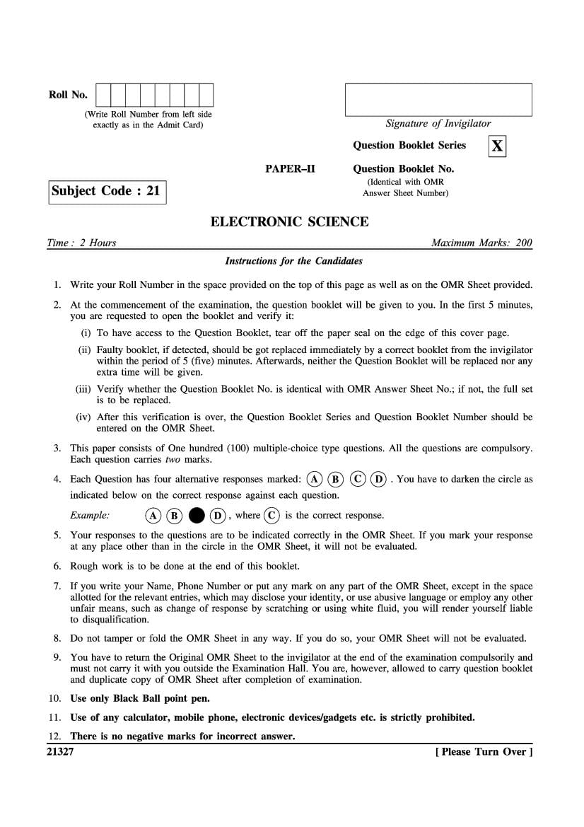
WB SET 2022 Question Paper Electronic Science
Finished viewing? Save it for later —
Download WB SET 2022 Question Paper Electronic Science (PDF · 20 pages)About WB SET 2022 Question Paper Electronic Science
WB SET 2022 Question Paper Electronic Science is available here for free download. Published by Default for Govt Jobs Exams, this question paper can be viewed online or downloaded as a PDF (20 pages). Candidates preparing for Govt Jobs Exams can use WB SET 2022 Question Paper Electronic Science to understand the exam pattern, the type of questions asked, and the overall difficulty level.
Frequently Asked Questions
How can I download WB SET 2022 Question Paper Electronic Science?
Open this page and click the Download button to save WB SET 2022 Question Paper Electronic Science as a PDF. It is completely free on AglaSem Docs.
Is WB SET 2022 Question Paper Electronic Science free to download?
Yes. WB SET 2022 Question Paper Electronic Science can be viewed online and downloaded as a PDF free of cost on AglaSem Docs.
How many pages does WB SET 2022 Question Paper Electronic Science have?
WB SET 2022 Question Paper Electronic Science contains 20 pages, which you can read online or download together as a single PDF.
Where can I find more Govt Jobs Exams study material?
You can find more Govt Jobs Exams question papers, sample papers, syllabus, and answer keys on AglaSem Docs.
WB SET 2022 Question Paper Electronic Science – Text
Read the full text of this question paper below — useful to quickly search, copy and reference the content online without downloading the PDF.
📄 View text version (14 pages)
Page 3
PAPER II
(ELECTRONIC SCIENCE)
1. According to Einstein relation, for any 5. The measured trans-conductance gm of an
semiconductor the ratio of diffusion constant to mobility NMOS transistor operating in the linear region is
of carriers plotted against the gate voltage VG at a constant drain
(A) depends upon the temperature of the voltage VD. Which of the following figures represents
semiconductor. the expected dependence of gm on VG?
(B) depends upon the type of the
semiconductor.
(C) varies with the lifetime of the
semiconductor. gm
(D) is a universal constant. (A)
VG
2. A zener diode works on the principle of
(A) tunneling of charge carriers across the
junction.
(B) thermionic emission.
(C) diffusion of charge carriers across the (B) gm
junction.
(D) hopping of charge carriers across the
junction.
VG
gm
3. A particular green LED emits light of wavelength
5490D. The energy bandgap of the semiconductor (C)
material used there is (Plank’s constant
–34
= 6·626 × 10 J–S)
(A) 2·26 eV
(B) 1·98 eV VG
(C) 1·17 eV
(D) 0·74 eV
gm
(D)
4. The threshold voltage of an n-channel MOSFET
can be increased by
(A) increasing the channel dopant VG
concentration.
(B) reducing the channel dopant concentration.
(C) reducing the gate oxide thickness.
(D) reducing the channel length.
[ Please Turn Over ]
Page 4
6. MOSFET can be used as a 10. The reverse saturation current in a p–n junction
(A) current controlled capacitor. diode operated below the breakdown voltage
(B) voltage controlled capacitor. (A) depends upon the magnitude of the reverse
bias.
(C) current controlled inductor.
(B) increases with the increase in device
(D) voltage controlled inductor.
temperature.
(C) decreases with the increase in device
temperature.
(D) independent of the nature of the
semiconductor used in the fabrication of
7. If ‘fr’ be resonant frequency and f is the the diode.
difference between two half power frequencies then Q
of the unloaded resistor is
(A) Q = f/fr
11. A tunnel diode
(B) Q = f × fr
(A) shows a differential negative resistance
(C) Q = fr/f
under proper forward bias.
(D) Q = 2fr/f
(B) shows a differential negative resistance
under reverse bias.
(C) is a very high power microwave source.
8. Vcc = 5V (D) is a four terminal device.
1K 1K 1K LED
12. Which method of thickness measurement
1K follows optical principle?
(A) Ellipsometer
S1 S2
(B) Screw gauge technique
(C) Ultrasonic thickness meter
(D) Profilometer
The LED
(A) emits light when both S1 and S2 are closed.
(B) emits light when both S1 and S2 are open. 13. Which etching technique does not include
(C) emits light when either S1 or S2 is closed. physical etching process?
(D) does not emit light; irrespective of the (A) Plasma etching
switch position. (B) Reactive ion etching
(C) Wet etching
(D) Sputter etching
14. Which lithorgraphy process has higher
9. The diffusion length of carriers depends on resolution?
(A) the shape of the semiconductor. (A) Photolithography
(B) the lifetime of the carrier alone. (B) e-beam lithography
(C) the mobility and the lifetime of the carrier. (C) ion beam lithography
(D) the mobility of the carrier alone. (D) X-ray lithography
Page 5
15. Which compounds are formed in etching of 20. The value of R required for maximum power
SiO2 using dry etching process with CF4 gas? transfer in the network shown below is
(A) SiF4, CO2 5 4
(B) O2, Si
(C) F2, O2 25V
(D) Si, F2 20 3A R
16. In 8086 microprocessor, one of the following
statements is not true:
(A) Coprocessor is interfaced in max mode. (A) 2
(B) Coprocessor is interfaced in min mode. (B) 4
(C) I/O can be interfaced in max/min mode. (C) 8
(D) Supports pipelining. (D) 16
17. If X(n) = XR(n) + jXi(n) is a complex sequence
whose Fourier transform is given as
X() = XR() + jXi(), then what is the value of XR()? 21. Thevenin equivalent voltage VTH and resistance
RTH of the following circuit are
(A) X R n Cosωn – X i n Sinωn 30 25
n0
(B) X R n Cosωn X i n Sinωn 5V +
– 20
n0
VTH, RTH
(C) X R n Cosωn X i n Sinωn 5A
n
(D) X R n Cosωn – X i n Sinωn (A) –100V, 75
n
(B) 155V, 55
(C) 155V, 37
18. Laplace transform of u(t) sin(at) — (D) 145V, 75
S
(A) a2 S 2
a
(B) a2 S 2 22. A 2-port resistive network satisfies the condition
2
(C) S 3 4
a2 S 2 AD B C . The Z11 of the network is
2 3
(D) a 2 a2 S 2 4
(A)
3
19. The Fourier series expansion of a periodic 3
(B)
function with half-wave symmetry contains only 4
(A) Sine terms 2
(C)
(B) Cosine terms 3
(C) Odd harmonics 3
(D)
(D) Even harmonics 2
[ Please Turn Over ]
Page 6
23. The circuit shown in the figure below is 26. The output voltage (V0) in volt of the following
reciprocal if is circuit is
2H
0.5V1
I1 1 I2
+–
+ + 3
2 –
+ V0
V1 V2
+ +
I1 –
3Sin t –
– – (V)
(A) 2
(A) –2 Sin t
(B) –2
(B) –2 Cos t
(C) 1
(C) –1·5 Sin t
(D) –1
(D) –1·5 Cos t
27. The value of output voltage V0, in the circuit
below is
+12V
24. Which of the following statements is not correct? 1k
(A) Multivibrators are non-sinusoidal
oscillators.
3V +
(B) Multivibrators can be classified as astable, –
monostable and bistable. V0
1k
(C) Multivibrators are purely sinusoidal
oscillators.
(D) Astable multivibrators have no stable state. 1k
(A) 3V
(B) 6V
(C) 1·5V
(D) 8V
25. A capacitively coupled amplifier has a midband
gain of 100 and upper 3-dB frequency is 10kHz.
Midband gain is reduced to 10 by applying negative 28. The breakdown voltage of a transistor with its
feedback. The upper half power frequency with base open is BVCEO and that with emitter open is
feedback in kHz will be BVCBO, then
(A) 0·1 (A) BVCEO = BVCBO
(B) 10 (B) BVCEO > BVCBO
(C) 100 (C) BVCEO < BVCBO
(D) 1 (D) BVCEO is not related to BVCBO.
Page 7
29. Ripple factor for a half-wave rectifier — 34. The op-amp circuit shown in the figure is a
(A) 1·21 filter. The type of filter and its cut-off frequency are
respectively
(B) 0·48
10k
(C) 0·11
(D) 0·99
10k
–
30. The desirable characteristics of a
trans-conductance amplifier are Vi +
(A) high input resistance and high output 1F
resistance. 1k
(B) high input resistance and low output
resistance.
(C) low input resistance and high output (A) High Pass; 1000 rad/sec.
resistance. (B) Low Pass; 1000 rad/sec.
(D) low input resistance and low output (C) High Pass; 10000 rad/sec.
resistance.
(D) Low Pass; 10000 rad/sec.
31. Efficiency of class A power amplifier is 35. A Boolean function is implemented with the
CMOS logic shown in the figure below. The output
(A) 25%
function Y of the circuit is
(B) 50% VDD
(C) 75%
(D) 100%
A D P-Network
B
32. In a multistage R–C coupled amplifier the
coupling capacitor
C
(A) limits the low frequency response.
(B) limits the mid frequency response.
Y
(C) does not effect the frequency response.
(D) blocks the dc components without affecting D
the frequency response.
A B C N-Network
33. A dc power supply has a no-load voltage of 30V
and a full-load voltage of 25V at a full-load current of
1A. Its output resistance and load regulation
respectively are (A) (A + B + C) D
(A) 5 and 20% (B) A B C D
(B) 25 and 20%
(C) ABC D
(C) 5 and 16·7%
(D) 25 and 16·7% (D) BC + AD
[ Please Turn Over ]
Page 8
36. Two ECL gates are cascaded. The voltage levels 39. The capacity of a PROM is 2K × 16. If it is
are VOH = – 0·96V, VOL = – 1·65V, VIH = – 1·105V expanded into 16K × 16, the number of address lines in
and VIL = – 1·475V. The low and high state noise the expanded memory will be
margins are (A) 16
(A) 0·37V and 0·69V (B) 14
(B) 0·545V and 0·51V (C) 12
(C) 0·175V and 0·145V (D) 10
(D) –2·065V and – 3·125V
37. The outputs of the 3 × 8 decoder are taken
through two logic gates as shown in the figure. The
outputs X and Y will be
0
1
2 X
A 3×8 3
B Decoder 4 40. The function F = A B C D can be
5 Y represented in canonical SOP form as
C 6
7
(A) m 2,3,5, 6, 7,8,12,14
(A) X = A BC + BC, Y = A + B (B) m 0,1, 3,5, 7,8,14,15
(B) X = A C + BC, Y = 1 (C) m 3, 4, 6, 7,8,9,13,14
(C) X = A, Y = 1 (D) m 1, 2, 4, 7,8,11,13,14
(D) X = A, Y = 0
38. A mod-N synchronous counter is shown in
figure below with T F/F and Q2 as MSB. If initially
Q0 = 0, Q1 = 0, Q2 = 0, the value of N is
Q2 T2 Q1 T1 Q0 T0
V
V
V
Q2 Q1 Q0
41. In BCD to seven segment display, the minimum
number and maximum number of outputs of the
decoder, that will be active one time are
(A) 8 (A) 1, 6
(B) 6 (B) 2, 7
(C) 5 (C) 3, 5
(D) 4 (D) 2, 8
Page 9
42. An 8 × 1 multiplexer with section lines B, C and 45. Which one of the following is true with respect
D is given below. The Boolean function Y implemented to CPLD and FPGA devices?
is (A) CPLD architecture offers greater
1 I0 flexibility.
0 I1 (B) FPGA devices have very complex
configurable logic blocks.
1 I2
A I3 (C) CPLD devices offer relatively lower
flexibility but more predictable timing
I4 Y characteristics.
0 I5 (D) FPGA devices offer relatively lower
I6 flexibility but more predictable timing
0 I7 characteristics.
S2 S1 S0
EN
46. Conversion time of an eight bit successive
B C D (LSB) approximation type A/D converter run by a 10MHz
clock would be
(A) m 1,3, 4, 6
(A) 12·75 S
(B) m 0, 2,3, 4,8,10,14 (B) 25·5 S
(C) 800 nS
(C) m 0, 3, 4,8,11,15 (D) 80 nS
(D) m 1,3,5, 7,9,15
47. Which one is sequencial access secondary
43. If spacing between the wires of a transmission storage device?
line is increased, its characteristic impedance will (A) Magnetic tape
(A) increase. (B) Hard Disk
(B) decrease. (C) Floppy Disk
(C) remains unaffected. (D) CD-ROM
(D) None of the above
44. The structural code for 4 bit adder in VHDL is 48. Which of the following is volatile memory?
given below: (A) SRAM
COMPONENT adder IS (B) Flash Memory
GENERIC (n : INTEGER : = 3); (C) EPROM
PORT (input : IN BIT _ VECTOR (n DOWN TO O); (D) EEPROM
OUTPUT : OUT BIT_VECTOR (n DOWN TO O);
END COMPONENT;
If it is required to convert this code into 8 bit 49. Peripheral devices that are found on
adder, the changed variable would be microcontroller chip does not include
(A) Component (A) Counter
(B) Input (B) USB port
(C) Output (C) Serial communication interface
(D) n (D) Parallel communication interface
[ Please Turn Over ]
Page 10
50. Identify the peripheral function that is provided 54. The largest number that can be processed by a
in microcontroller by a pulse which modulator followed microprocessor in a single operation is determined by
by a filter. the size of which bus?
(A) A/D converter
(A) External data bus
(B) D/A converter
(B) Internal data bus
(C) Timer
(D) Counter (C) Address bus
(D) Control bus
51. A 8 bit microcontroller has an external RAM in
the memory map from 8000H to 9FFFH. The no. of 55. The synchronization between microprocessor
bytes that this RAM can store is and memory is done by
(A) 8193 (A) ALE signal
(B) 8192 (B) HOLD signal
(C) 8191 (C) READY signal
(D) 8000 (D) HLDA signal
52. Consider the following set of instructions:
56. The memory device has both high density and
MVI A, BYTE 1 high speed access and in-circuit electrical erasbility
RLC feature is
MOV B, A (A) EEPROM
RLC (B) UV EPROM
RLC (C) Cache Memory
ADD B
(D) Flash Memory
If BYTE1 = 07H, then the content of A after the
execution of the program will be
57. In quenched domain mode, the period of
(A) 46H microwave oscillation () is related with the domain
(B) 70H transit time (T) as
(C) 38H (A) = T
(D) 68H (B) < T
(C) = T/2
53. A set of 8085 instruction is given by
(D) > T
XRA A
MVI B, 4AH
58. An open-ended, lossless transmission line of
SUI 4FH length 5 km has a phase shift constant, = /10
ANA B radian/km and a characteristic impedance of 500 .
HLT The input impedance at the mid-point of this line
The contents of registers A and B are respectively in will be
(A) 05, 4A (A) 250
(B) 4F, 00 (B) – j500
(C) B1, 4A (C) – j125
(D) 00, 4A (D) j500
Page 11
59. The characteristic impedance (Z o ) of a 63. A hollow metallic waveguide with rectangular
transmission line can be expressed as (here, R, L, G, C cross-section of 3cm × 2cm will have a ratio of cut-off
are primary constants of the transmission line) frequencies for TE10 and TE01 modes equal to
(A) RG (A) 1 : 2
(B) 2 : 1
R jL
(B)
G jC (C) 2 : 3
(D) 1 : 3
R 1
jC
(C)
G j L
64. A two-cavity Klystron amplifier is operated
G 1
jC with a dc accelerating voltage of 100 volts and it
(D)
R jL amplifies a microwave signal of frequency 3 GHz. The
buncher gap width is 1mm. The beam coupling
coefficient of the buncher cavity is
60. The diagonal elements of a microwave magic-T
must be (A) 0·57
(A) 1, 0, 0, 1 (B) 0·82
(B) 1, 1, 1, 1 (C) 0·75
(C) 0, 1, 1, 0 (D) 0·63
(D) 0, 0, 0, 0
61. The continuity equation . J 0 65. The characteristic polynominal of a system is
t
expresses the conservation of q(s) = 2s5 + s4 + 4s3 + 2s2 + 2s + 1
(A) Energy The system is
(B) Power (A) stable
(C) Momentum (B) marginally stable
(D) Charge
(C) unstable
(D) oscillatory
62. A linear array of 10 half-wave dipole antennas
with an inter-element spacing of one wavelength directs
its maximum radiation in a direction perpendicular to
the line of the array. The width of the principal lobe of
66. A conventional cylindrical magnetron is operated
the array in radian, when the antenna elements are fed
with dc anode voltage of 2000 volt. The cathode has a
in phase by a microwave signal of frequency 1GHz,
radius of 5 cm and the anode radius measured from the
will be
cathode centre is 10 cm. The cut-off magnetic field of
(A) 0·2
this magnetron in milliweber/m2 is
(B) (A) 1
3
(C) 0·1 (B) 4
(C) 9
(D)
5 (D) 2
[ Please Turn Over ]
Page 12
67. If the closed loop transfer function of a control 72. In certain cases circular waveguide is the better
choice than a rectangular waveguide, because of
system is given as T ( S ) S5 , then it is
(S 2)( S 3) (A) smaller cross-section.
(B) lower attenuation.
(A) unstable system.
(C) freedom from spurious modes.
(B) an uncontrollable system. (D) higher cut-off frequency.
(C) a minimum phase system.
(D) a non-minimum phase system.
73. The relationship between the phase velocity vp
and group velocity vg in a waveguide is
(A) vp = vg
2
68. The maximum range of a radar does not depend (B) vp . vg = c /2
on the following: (C) vp . vg = c2
(A) Gain of the transmitting antenna. (D) vp . vg = c
(B) Power radiation of the transmitting
antenna.
74. Intrinsic impedance is given by
(C) Area of the target.
(D) Medium through which the wave is
propogating. (A)
(B)
69. Helical antenna is used for satellite tracking
because of its (C)
(A) circular polarization
(B) broad bandwidth (D)
(C) good front to back ratio
(D) small size
75. If a right-handed circularly polarized wave is
incident normally on a plane perfect conductor, then
the reflected wave will be
70. If the minimum range of a radar is to be doubled, (A) right-handed circularly polarized.
the peak power has to be increased by a factor of (B) left-handed circularly polarized.
(A) 2 (C) elliptically polarized with a tilt angle of
(B) 4 45º.
(C) 8 (D) horizontally polarized.
(D) 16
76. In a transmission line with L R and
C G , phase constant is proportional to
71. The blind speed of an MTI radar can be avoided (A)
by changing the
(B) 2
(A) carrier frequency
(B) antenna rotation rate (C)
(C) pulse repetition frequency
(D) transmitted power (D) 1
Page 13
77. The input impedance of a short circuited lossless 82. In amplitude modulation, the modulation
transmission line quarter wave long is envelope has a peak value which is double the
(A) purely reactive. unmodulated carrier value. What is the value of the
modulation index?
(B) purely resistive.
(A) 25%
(C) infinite.
(B) 50%
(D) dependent on the characteristic impedance
of the line. (C) 75%
(D) 100%
78. The frequency of oscillation of a Klystron depends 83. The signal m(t) = cos2000t + 2cos4000t is
on multiplied by the carrier c(t) = 100cos2fct where
fc = 1MHz to produce the DSB signal. The expression
(A) cavity dimension
for the upper side band (USB) signal is
(B) dc voltage
(A) 100cos(2(fc + 1000)t) + 200cos(2(fc + 200)t)
(C) distance between the two cavities
(B) 100cos(2(fc – 1000)t) + 200cos(2(fc – 2000)t)
(D) repeller voltage
(C) 50cos(2(fc + 1000)t) + 100cos(2(fc + 2000)t)
(D) 50cos(2(fc – 1000)t) + 100cos(2(fc – 100)t)
79. Gallium arsenide is preferred to silicon for use
in Gunn diode because it has 84. A signal with 3kHz bandwidth is sampled with
Nyquist rate and quantized with 128 level quantizer in
(A) lower noise at high frequencies. a PCM system. What will be the corresponding
(B) better frequency stability. minimum transmission bandwidth?
(C) high ion mobility. (A) 42 kHz
(D) suitable empty energy band which silicon
(B) 21 kHz
does not have.
(C) 84 kHz
(D) 384 kHz
80. Periodic permanent magnet focussing is used
with TWTs to 85. The bandwidth efficiency of QPSK modulation
(A) improve electron bunching. is doubled compared to BPSK modulation. The
(B) allow pulsed operation. probability of bit error for QPSK is
(C) allow coupled-cavity operation at highest (A) same as BPSK
frequencies. (B) double of BPSK
(D) avoid the bulk of an electromagnet. (C) half of BPSK
(D) one-fourth of BPSK
81. For an FM station transmitting at 100MHz, the 86. In an optical fiber link of 15 km, the optical
frequency deviation is 75 kHz. Find the approximate power connected at the input is 50 mw. The optical
bandwidth required for transmission of voice signals power measured at the output of the fiber is 8 mw. The
(0 – 3kHz). attenuation of the fiber in dB/km is
(A) 78 kHz (A) 2·5
(B) 156 kHz (B) 0·75
(C) 175 kHz (C) 0·53
(D) 158 kHz (D) 0·14
[ Please Turn Over ]
Page 14
87. A mixer stage has a noise figure of 20dB. This 92. An SCR is considered to be a semi-controlled
mixer stage is preceded by an amplifier which has a device because
noise figure of 9 dB and an available power gain of (A) it can be turned off but not on with a Gate
15 dB. The overall noise figure referred to the input is pulse.
(A) 11·07 (B) it conducts only during one half cycle of
(B) 18·23 an alternating current wave.
(C) 56·48 (C) it can be turned on but not off with a Gate
(D) 97·38 pulse.
(D) it can be found on only during one half
cycle of an AC.
88. The Nyquist sampling rate for the signal
g(t) = 10cos (50t)cos2(150t), where ‘t’ is in seconds is
(A) 150 samples per second
(B) 350 samples per second 93. An SCR has half cycle surge current rating of
(C) 300 samples per second 3000A for 50 Hz supply. One cycle surge current will
(D) 200 samples per second be
(A) 1500A
(B) 6000A
89. In a PCM system, if the quantization levels are (C) 2121·32A
increased from 2 to 8, the relative bandwidth (D) 4242·64A
requirement will
(A) remain same.
(B) be tripled.
(C) be doubled.
94. A piezoelectric transducer has a voltage source
(D) become four times.
of 12V with an internal impedance of 12M. It is
connected to a digital oscilloscope with an input
impedance of 12 M directly. The voltage measured
90. An InGaAs photodiode has a quantum efficiency
of 90% at a wavelength of 1550nm. The responsivity by the oscilloscope is
of the photodiode is (A) 3V
(A) 2·25 A/W (B) 6V
(B) 1·12 A/W (C) 12V
(C) 0·92 A/W
(D) 24V
(D) 0·56 A/W
91. The tuning current in a DFB laser operating at
1550nm causes a change in effective refractive index 95. A n-type semiconductor strain gauge has a
of 0·85%. If the source spectral width is 0·04nm for nominal resistance of 1k and gauge factor of –100.
2Gbps signal, the number of channels that can be The resistance of the gauge when a compressive strain
operated for DWDM system is of 100 m/m is applied, is
(A) 27 (A) 1100
(B) 33 (B) 1010
(C) 52 (C) 990
(D) 65 (D) 900
Page 15
96. A copper-iron thermocouple has its measuring 98. A square wave signal is observed on the
junction kept at 110ºC and the reference junction at the oscilloscope to have one cycle measured 5cm at a
temperature of 28ºC. The temperature emf horizontal sweep rate of 25 s/cm. The signal frequency
characteristics of iron-constantan and copper- is
constantan are EI–C = 53TV and EC–C = 43TV, (T is (A) 125 Hz
in ºC), at 0ºC. The emf developed in the thermocouple
(B) 4 kHz
would be
(C) 8 kHz
(A) 1100 V
(D) 16 MHz
(B) 2800 V
(C) 720 V
(D) 1380 V 99. A DIAC is equivalent to a
(A) triac with two gates
(B) diode and two resistors
(C) pair of SCRs
(D) pair of four layer SCRs
97. A spectrum analyser displays
(A) peak to peak amplitude of modulating
signal. 100. Which instruction cannot force the 8086
processor out of ‘halt’ state?
(B) different frequency amplitudes with
respect to time. (A) Interrupt request
(C) Lissajous figures. (B) Reset
(D) different signal amplitudes with respect to (C) Both interrupt request and reset
frequency. (D) Hold
Page 16
Space for Rough Work
Document Details
| Board / Org | Default |
| Exam | Govt Jobs Exams |
| Type | Question Paper |
| Pages | 20 |
| Updated | 30 Apr 2026 |