MAHA SET 2024 Paper II Electronic Science Set A Question Paper
Finished viewing? Save it for later —
Download MAHA SET 2024 Paper II Electronic Science Set A Question Paper (PDF · 24 pages)About MAHA SET 2024 Paper II Electronic Science Set A Question Paper
MAHA SET 2024 Paper II Electronic Science Set A Question Paper is available here for free download. Published by Maharashtra Exams for MAHA SET, this question paper can be viewed online or downloaded as a PDF (24 pages). Candidates preparing for MAHA SET can use MAHA SET 2024 Paper II Electronic Science Set A Question Paper to understand the exam pattern, the type of questions asked, and the overall difficulty level.
Frequently Asked Questions
How can I download MAHA SET 2024 Paper II Electronic Science Set A Question Paper?
Open this page and click the Download button to save MAHA SET 2024 Paper II Electronic Science Set A Question Paper as a PDF. It is completely free on AglaSem Docs.
Is MAHA SET 2024 Paper II Electronic Science Set A Question Paper free to download?
Yes. MAHA SET 2024 Paper II Electronic Science Set A Question Paper can be viewed online and downloaded as a PDF free of cost on AglaSem Docs.
How many pages does MAHA SET 2024 Paper II Electronic Science Set A Question Paper have?
MAHA SET 2024 Paper II Electronic Science Set A Question Paper contains 24 pages, which you can read online or download together as a single PDF.
Where can I find more MAHA SET study material?
You can find more MAHA SET question papers, sample papers, syllabus, and answer keys on AglaSem Docs.
MAHA SET 2024 Paper II Electronic Science Set A Question Paper – Text
Read the full text of this question paper below — useful to quickly search, copy and reference the content online without downloading the PDF.
📄 View text version (25 pages)
Page 1
MAHA SET 2024 Paper
II Electronic Science Set
A Question Paper
EXAM YEAR TYPE
MAHA SET 2024 Question Paper
Notes · Sample Papers · Previous Year Papers · Mock Tests
Page 2
. s e
em l a
as ag
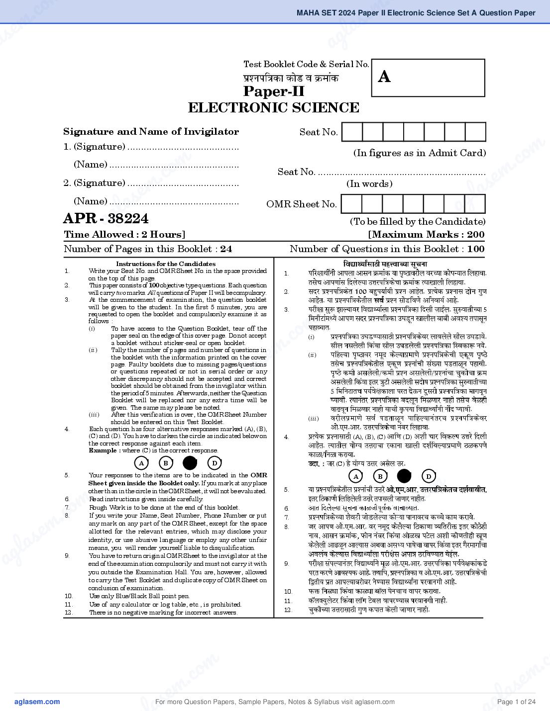
Test Booklet Code & Serial No.
A
ELECTRONIC SCIENCE
m
Signature and Name of Invigilator Seat No.
om . co
1. (Signature) .........................................
(In figures as in Admit Card)
.c e m
(Name) ................................................
m a s
Seat No. ..............................................................
s e g l
2. (Signature) ......................................... (In words)
gl a
(Name) ................................................
a
APR -a38224
OMR Sheet No.
(To be filled by the Candidate)
Time Allowed : 2 Hours] [Maximum Marks : 200
Number of Pages in this Booklet : 24 Number of Questions in this Booklet : 100
Instructions for the Candidates
1. Write your Seat No. and OMR Sheet No. in the space provided 1.
on the top of this page.
2. This paper consists of 100 objective type questions. Each question
will carry two marks. All questions of Paper II will be compulsory. 2.
3. At the commencement of examination, the question booklet
m
will be given to the student. In the first 5 minutes, you are 3.
co
requested to open the booklet and compulsorily examine it as
.
follows :
(i) To have access to the Question Booklet, tear off the
em
paper seal on the edge of this cover page. Do not accept (i)
las
a booklet without sticker-seal or open booklet.
(ii) Tally the number of pages and number of questions in
the booklet with the information printed on the cover (ii)
ag
page. Faulty booklets due to missing pages/questions
or questions repeated or not in serial order or any
other discrepancy should not be accepted and correct
booklet should be obtained from the invigilator within
the period of 5 minutes. Afterwards, neither the Question
Booklet will be replaced nor any extra time will be
given. The same may please be noted.
(iii) After this verification is over, the OMR Sheet Number
(iii)
should be entered on this Test Booklet.
4. Each question has four alternative responses marked (A), (B),
(C) and (D). You have to darken the circle as indicated below on 4. (A), (B), (C) (D)
the correct response against each item.
Example : where (C) is the correct response.
A B D (C)
m
c. o
5. Your responses to the items are to be indicated in the OMR A B D
m
Sheet given inside the Booklet only. If you mark at any place
c. o
other than in the circle in the OMR Sheet, it will not be evaluated. 5.
e m
6. Read instructions given inside carefully.
em s
7. Rough Work is to be done at the end of this booklet. 6.
la
8. If you write your Name, Seat Number, Phone Number or put 7.
s ag
any mark on any part of the OMR Sheet, except for the space
la
8.
allotted for the relevant entries, which may disclose your
g
identity, or use abusive language or employ any other unfair
a
means, you will render yourself liable to disqualification.
9. You have to return original OMR Sheet to the invigilator at the
end of the examination compulsorily and must not carry it with 9.
you outside the Examination Hall. You are, however, allowed
to carry the Test Booklet and duplicate copy of OMR Sheet on
conclusion of examination.
10.
10. Use only Blue/Black Ball point pen.
11.
11. Use of any calculator or log table, etc., is prohibited.
12. There is no negative marking for incorrect answers. 12.
m . c
c. o s e m
m a
se
For more Question Papers, Sample Papers, Notes & Syllabus visit
g l
Page 1 of 24
Page 3
For more Question Papers, Sample Papers, Notes & Syllabus visit Page 2 of 24
Page 4
. s e
em l a
as a g
Electronic Science
Paper II
m
co
Time Allowed : 120 Minutes] [Maximum Marks : 200
om .
Note : This Paper contains Hundred (100) multiple choice questions. Each question
.c e m
carrying Two (2) marks. Attempt All questions.
m
e l a s
1.
a s
l diode in semiconductor
What is the main purpose of a 3. What type of backlighting is
ag
ag
Schottky commonly used in LCD displays for
applications ? improved color reproduction ?
(A) Voltage regulation (A) Fluorescent backlighting
(B) Incandescent backlighting
(B) High-speed switching
o m
.c (D) OLED backlighting
(C) LASER backlighting
(C) Temperature sensing
e m
(D) Power amplification
l a s
2. What is the primary advantage of a g 4. What is the purpose of connecting
a resistor in series with a Zener diode
using a Gallium Nitride (GaN)
in a voltage regulator circuit ?
semiconductor over traditional
(A) To increase the breakdown
silicon in power electronics ?
voltage
m
m c. o
(A) Higher electron mobility
c. o (B) Lower bandgap m
(B) To limit the forward bias
s e
s em la
current
gla ag
a
(C) Greater thermal stability (C) To decrease the reverse bias
(D) Improved resistance to voltage
radiation (D) To provide mechanical stability
3 [P.T.O.
m . c
c. o s e m
m a
se
For more Question Papers, Sample Papers, Notes & Syllabus visit
g l
Page 3 of 24
Page 5
in the electronic structure of
semiconductor device is known for
graphene ?
its ability to confine charge carriers
(A) They represent the valence and
in all three dimensions ?
conduction bands
(A) Quantum wells (B) They indicate the presence of a
bandgap
(B) Quantum wires
(C) They show the dispersion
(C) Quantum dots relation of electrons
(D) Quantum cascade devices (D) They enhance the magnetic
properties of graphene
6. What is the role of the series
8. How does the chirality of a carbon
resistance in the I-V characteristics
nanotube affect its electronic
of a solar cell ? properties ?
(A) To reduce the open-circuit (A) It determines whether the
nanotube is metallic or
voltage
semiconducting
(B) To decrease the short-circuit
(B) It affects the mechanical
current strength of the nanotube
(C) To limit the current flow in the (C) It influences the thermal
conductivity of the nanotube
external circuit
(D) It is unrelated to the electronic
(D) To maximize the fill factor
properties of nanotubes
4
For more Question Papers, Sample Papers, Notes & Syllabus visit Page 4 of 24
Page 6
. s e
em l a
as a g
9. How does ZnO exhibit both 11. Which of the following statements
is true in case of CMOS fabrication ?
m
co
semiconducting and piezoelectric
c om m .
(A) Fabrication of n-mos transistor
. e
properties simultaneously ?
em a
requires few additional steps
l s
a s
l concentration
(A) Through the manipulation of
ag
compared to p-MOS transistor
ag
doping
(B) Fabrication on n-MOS is same
(B) Due to its wurtzite crystal as that of p-MOS transistor
structure (C) Fabrication on n-MOS is
different from that of p-MOS
(C) By controlling the synthesis
transistor
m
c. o (D) Fabrication of p-MOS transistor
temperature
(D) It does not possess piezoelectric em
a s
requires few additional steps
g l
a
compared to n-MOS transistor
properties
12. EDAX is a technique used in
10. In an LED, what is the function of
conjunction with SEM for :
the p-n junction ?
(A) Energy dispersive analysis of
(A) To modulate the intensity of X-rays
o m
m c
electrons excited. by X-rays
light (B) Energy levels occupied by
c. o (B) To amplify the input signal s em
s em a
(C) Electron ldiffraction
g
la X-ray aexcitations
analysis of
ag
(C) To emit light when forward-
biased
(D) Obtaining higher magnification
(D) To store electrical charge levels
5 [P.T.O.
m . c
c. o s e m
m a
se
For more Question Papers, Sample Papers, Notes & Syllabus visit
g l
Page 5 of 24
Page 7
by technique known as ................
(A) Control Circuit Design
(A) Selective deposition of field-
(B) Central Core Database
oxide isolation
(B) Local Oxidation of Silicon (C) Charge-Coupled Device
(C) Etched field-oxide isolation or (D) Composite Camera Device
Local Oxidation of Silicon
17. As die size shrinks. the complexity
(D) Reverse biased pn junction
of making the photomasks ...........
14. The gate delay is proportional to :
(A) increases
(A) Ron.Cg
(B) decreases
(B) Rs.Cds
(C) remains the same
(C) Rd.Cgs
(D) cannot be determined
(D) Ron.Cox
18. The minimum width of n-diffusion
15. At threshold voltage, the surface
potential is : and p-diffusion layer should be :
(A) Negative Fermi potential (A) 3
(B) Fermi potential (B) 2
(C) 2 Fermi potential (C)
(D) –2 Fermi potential
(D) 4
6
For more Question Papers, Sample Papers, Notes & Syllabus visit Page 6 of 24
Page 8
. s e
em l a
as a g
19. Where are the silicon wafers placed 22. In a parallel resonant circuit, the
m
in the reaction chamber for the impedance is minimum at :
om
epitaxial growth process ?
. co
.c e m
(A) Resonant frequency
(A) Cup
e m l a s
l a s (B) Half the resonant frequency
ag
ag
(B) Boats
(C) Double the resonant frequency
(C) Ingots
(D) Crucible (D) Quarter the resonant frequency
20. As per lambda design rules for wires 23. Norton’s equivalent current source
minimum width of metal 2 is ............. is connected in :
m
c. o (A) Series with the load
and separation between two metal
s em
2 layers .....................
g l a (B) Parallel with the load
a
(A) 4 lambda, 4 lambda
(B) 3 lambda, 3 lambda (C) Series with the source
(C) 4 lambda, 3 lambda (D) Parallel with the source
(D) 3 lambda, 4 lambda 24. The unit step response of a first-
m
c. o
21. In an AC circuit, the power factor order system exhibits :
m
c. o (A) Voltage angle m
is the cosine of the :
s e
(A) Oscillations
s em la
gla ag
(B) Exponential rise
a
(B) Current angle
(C) Exponential decay
(C) Phase angle
(D) Sine wave behaviour
(D) Resistance angle
7 [P.T.O.
m . c
c. o s e m
m a
se
For more Question Papers, Sample Papers, Notes & Syllabus visit
g l
Page 7 of 24
Page 9
in network analysis ?
role of the Hurwitz criterion ?
(A) To represent the step response
(A) To determine the stability of a
of a system
control system
(B) To visualize the frequency
(B) To check the realizability of a response of a system
network
(C) To analyze the transient
(C) To analyze the frequency behavior of a circuit
response of a circuit (D) To plot the time domain
behavior of a network
(D) To evaluate the accuracy of
28. What is the purpose of the Smith
numerical methods in solving
predictor in control system design ?
circuits
(A) To compensate for time delays
26. The Smith chart is primarily used
in the system
for the analysis of :
(B) To enhance the transient
(A) Transmission lines response of the system
(C) To reduce overshoot in the step
(B) Filters
response
(C) Log Amplifiers
(D) To improve the frequency
(D) Oscillators response of the system
8
For more Question Papers, Sample Papers, Notes & Syllabus visit Page 8 of 24
Page 10
. s e
em l a
as a g
29. The concept of ‘‘duality’’ in network 31. What does the hFE value represent
in the common-emitter
m
synthesis refers to :
om . co
configuration ?
.csignals in a system e m
(A) The relationship between input
em s
(A) Reverse current transfer ratio
s
and output
g l a
la interchangeability of a
(B) Output impedance
g
aresistors and capacitors in a
(B) The
(C) Voltage gain
(D) Forward current transfer ratio
network
32. How does the Schmitt trigger
(C) The dual representation of a eliminate the erratic operation in the
network in terms of nodes and op-amp comparator ?
m
c. o (A) By reducing the sensitivity
branches
(D) The ability of a network to em
la s (B) By introducing negative
a g
exhibit both series and parallel feedback
elements (C) By using positive feedback
30. Consider the signal x[n] = 2n u[n] (D) By increasing the reference
voltage
having Z-transform as X(z) with
ROC R. The inverse Z transform 33. What is the main disadvantage of
m
c. o
half-wave rectifier compared to full
m
for X (2z) will be :
c. o (A) u[n] e m
wave rectifier ?
em la s
s ag
(A) Higher cost
l a
ag
(B) 2n u[n] (B) Lower efficiency
(C) 4u u[n] (C) Limited voltage output
(D) 22n u[n] (D) More complex circuitry
9 [P.T.O.
m . c
c. o s e m
m a
se
For more Question Papers, Sample Papers, Notes & Syllabus visit
g l
Page 9 of 24
Page 11
34. In any circuit connections, what is
in the context of PLLs :
the biasing direction for the emitter (A) Phase noise is the phase
deviation between the reference
and collector of a transistor ?
and feedback signals
(A) Both are forward biased (B) Phase noise is the undesirable
random fluctuations in the
phase of the output signal
(B) Both are reverse biased
(C) Phase noise is the intentional
(C) Emitter is forward, and collector modulation of the VCO
frequency
is reverse biased
(D) Phase noise is the difference in
phase between the input and
(D) Emitter is reverse, and collector output of the phase comparator
is forward biased 37. Oscillators operate on the principles
of .............
35. In a CE configuration, an emitter (A) Signal feedthrough
(B) Positive feedback
resistor is used for ...............
(C) Negative feedback
(A) Stabilization (D) Ultra high gain
38. Following circuits can be used as
(B) AC signal bypass voltage to frequency converter :
(A) Astable multivibrator
(C) Collector bias (B) Crystal oscillator
(C) Schmitt trigger
(D) Higher gain
(D) CE amplifier
10
For more Question Papers, Sample Papers, Notes & Syllabus visit Page 10 of 24
Page 12
. s e
em l a
as a g
39. What is the advantage of using IC 42. What does SPLD stand for in the
context described ?
m
LM725 ?
om
(A) Simple Programming Logic
. co
.c e m
(A) Very high gain
m a s
Device
s e g l
a a
(B) Very high BW
gl CMRR
(B) Sequential Programmable Logic
(C) aHigh Device
(D) High slew rate (C) Systematic PLD
(D) Structured Programming and
40. Which of the following units is used
Logic Device
to convert square wave into
m
43. Which statement accurately
c. o describes the programming of an
triangular wave ?
(A) Differentiator
s em FPGA ?
g l a
(B) Integrator
a (A) FPGA programming
permanent and cannot be
is
(C) Schmitt trigger
changed.
(D) Monoshot multivibrator
(B) FPGA programming is done
41. How is the complement nature of using machine code
NOR represented in its graphic
o m
c
(C) FPGA programming is done
m using hardware. description
c. o em or schematic
symbol ?
em (A) A small square a s
s entry gl
languages (HDLs)
l a a
ag (B) A small triangle
(D) FPGA programming is only
(C) A small circle possible in a controlled
(D) A small diamond laboratory environment
11 [P.T.O.
m . c
c. o s e m
m a
se
For more Question Papers, Sample Papers, Notes & Syllabus visit
g l
Page 11 of 24
Page 13
Network in CPLD ? of a ripple counter with ‘n’ flip-flop
(A) It synchronizes all clock signal is :
in the devices (A) 2 n
(B) It is responsible for configuring
(B) n
the entire devices
(C) 2n – 1
(C) It has no impact on timing
constraints (D) n 2
(D) It is used for power 48. Output values of Moore type FSM
consumption are determined by its ..............
45. For design of 16 : 1 MUX how many (A) Clock input
select lines are required ?
(B) Current state
(A) 1
(C) Input values
(B) 2
(D) Output values
(C) 3
49. VHDL ..................... represents a
(D) 4
component's external behavior and
46. A decoder converts ‘n’ inputs to ......... interface.
outputs.
(A) Signal
(A) n
(B) Port
(B) n 2
(C) Entity
(C) 2 n
(D) Architecture
(D) n n
12
For more Question Papers, Sample Papers, Notes & Syllabus visit Page 12 of 24
Page 14
. s e
em l a
as a g
50. Race Around condition can be 53. What is the status of the carry,
avoided in digital logic circuits
m
auxiliary carry and parity flags after
m . co
using :
c. o
executing following instructions ?
e m
em a s
(A) Shift register MOV A,#9C
(B) Full sadder g l
g la a
ADD A.#64H
(C) aAND gate (A) CY = 0, AC = 0, P = 0
(B) CY = 1, AC = l, P = 0
(D) Master slave JK flip-flop
(C) CY = 0, AC = 1, P = 0
51. The configuration in which each
(D) CY = l, AC = l, P = 1
LED receives operating current of
m
c. o that is being used as the clock source
8 mA from power supply while the 54. What is the frequency of the clock
em for the timer ?
port lines sink the current on each
port line is :
l a s
(A) driver configuration a g (A) some externally applied
frequency f’
(B) common anode configuration
(B) controller’s crystal frequency f
(C) common cathode configuration
(C) controller’s crystal frequency/12
(D) buffer configuration
(D) externally applied frequency/12
o m
c
52. If no key is pressed microcontroller
m8051 port will read : .bit wide.
c. o
55. In 8086 microprocessor, the address
e m
em (A) 0 (A) 12 bit la
s
bus is .........................
las a g
ag (B) 1 (B) 10 bit
(C) NC (C) 16 bit
(D) 7 (D) 20 bit
13 [P.T.O.
m . c
c. o s e m
m a
se
For more Question Papers, Sample Papers, Notes & Syllabus visit
g l
Page 13 of 24
Page 15
grouping ....................... .
microcontroller at least consist of :
(A) BH & BL
(A) CPU, ROM, I/O ports and
(B) CH & CL
Timers
(C) AH & AL
(D) DH & DL (B) RAM, ROM, I/O ports and
57. A 20-bit address bus allows access Timers
to a memory of capacity :
(C) CPU, RAM, I/O ports and
(A) 1 MB
Timers
(B) 2 MB
(C) 4 MB (D) CPU, RAM, ROM, I/O ports and
(D) 8 MB Timers
58. What is the Address (SFR) for 61. A non-conducting sphere has
TCON, SCON, SBUF, PCON and
uniform charge density in it. The
PSW respectively ?
electric field at a point inside the
(A) 88H, 98H, 99H, 87H, 0D0H
sphere will be .................
(B) 98H, 99H, 87H, 88H, 0D0H
(C) 0D0H, 87H, 88H, 99H, 98H (A) Zero
(D) 87H, 88H, 0D0H, 98H, 99H (B) Only due to the charge inside
59. In 8051 which interrupt has highest that point
priority ?
(C) Only due to the charge outside
(A) IE1
(B) TF0 that point
(C) IE0 (D) Due to the entire charge of the
(D) TF1 sphere
14
For more Question Papers, Sample Papers, Notes & Syllabus visit Page 14 of 24
Page 16
. s e
em l a
as a g
62. What happens to the current in a 65. Which component of the electric field
coil while accelerating a magnet intensity is always continuous at the
m
m . co
inside it ? boundary ?
(A) Increases co m
m . s e
e a
(A) Tangential
a s g l
l a
(B) Decreases
g
(B) Normal
a
(C) Remains constant
(C) Horizontal
(D) Reverses
(D) Vertical
63. In an electromagnetic wave, the
electric field of amplitude 6.2 V/m 66. Calculate the skin depth of a
oscillates with a frequency of material with attenuation constant
m
c. o (A) 2
2.4 × 10 10 Hz. Estimate energy of 2 units.
em
density of the wave :
l a s
g
( 8.85 10 –12 C 2 / Nm 2 )
a
(B) 1
(A) 1.4 × 10⁻¹⁰ J/m3
(C) 0.5
(B) 2.4 × 10⁻¹⁰ J/m3
(D) 4
(C) 3.4 × 10⁻¹⁰ J/m3
(D) 4.4 × 10⁻¹⁰ J/m3 67. The expression for velocity of a wave
m
64. The ratio of conduction to in the conductor is :
m c. o
c. o referred to as : m
displacement current density is
s e
(A) V 2 /
s em (A) Attenuation constant 2 la
la ag
(B) V
ag (B) Propagation constant
(C) V 2 /
(C) Loss tangent
(D) V 2
(D) Dielectric constant
15 [P.T.O.
m . c
c. o s e m
m a
se
For more Question Papers, Sample Papers, Notes & Syllabus visit
g l
Page 15 of 24
Page 17
circuited and open circuited lines will modulation technique used for
be : transmitting :
(A) 0 (A) digital data over analog
(B) 1 channel
(C) –1 (B) analog data over digital
(D) channel
69. In a good conductor the phase (C) binary signals only
relation between the tangential
(D) FM signals
components of electric E and the
72. A PLL maintains lock by comparing :
magnetic field H is as follows :
(A) E and H are in phase (A) The phase of two signals
(B) E and H are out of phase (B) The frequency of two signals
(C) H leads E by 90 (C) The amplitude of two signals
(D) E leads H by 45 (D) The amplitude of input signal
70. Consider a transmission line of with a fixed threshold
characteristic impedance 50 ohm.
73. To increase level of very weak radio
Let it be terminated at one end by
signals from an antenna, you would
+ j50 ohm. The VSWR produced by use :
it in the transmission line will be :
(A) an RF oscillator
(A) 1
(B) an audio oscillator
(B) 0
(C) an RF amplifier
(C) Infinity
(D) + j (D) an audio amplifier
16
For more Question Papers, Sample Papers, Notes & Syllabus visit Page 16 of 24
Page 18
. s e
em l a
as a g
74. Which is the true statement about 76. Which is called as on-off keying ?
m
frequency deviation in frequency (A) Frequency shift keying
modulation ?
om . co
c deviation m
(B) Uni-polar PAM
m . s e
e l a
(A) frequency is (C) Amplitude shift keying and
l a s ag
g
proportional to carrier signal Uni-polar PAM
afrequency (D) Phase shift keying
(B) frequency deviation is 77. Which of the following technology
distributes the coverage of the cell
proportional to amplitude of
and extends the cell boundary to
carrier signal
hard-to-reach places ?
o m
(C) frequency deviation is
.c (B) Cell splitting
(A) Sectoring
e m
proportional to modulating
frequency
l a s
(D) frequency deviation a g is
(C) Micro cell zone concept
(D) Scattering
proportional to amplitude of
78. A planar LED is fabricated from
modulating signal
GaAs is having a optical power
75. The equivalent noise temperature of emitted, which is 0.018% of optical
m
a network given the noise figure of power generated internally which is
m c. o
c. o (A) T0 (F – 1)
0.6 P. Determine external power
m
the network or system is :
s e
em
efficiency :
s g la
la a
(A) 0.18%
ag (B) T0 (F + 1)
(B) 0.32%
(C) T0 (F) (C) 0.65%
(D) T0/F (D) 0.9%
17 [P.T.O.
m . c
c. o s e m
m a
se
For more Question Papers, Sample Papers, Notes & Syllabus visit
g l
Page 17 of 24
Page 19
30 m sec at 50ºC. Its turn-off time
the total fiber attenuation per unit
at 100º is :
length is ................ method.
(A) same
(A) Frank
(B) 15 m sec
(B) Cut-off
(C) 60 m sec
(C) Cut-back
(D) 100 m sec
(D) OSA
82. A six pulse thyristor rectifier bridge
80. Global Sensor Network is built for : is connected to a balanced 50 Hz
three-phase ac source. Assuming
(A) Reducing cost and time for
that the dc output current of the
development
rectifier is constant, the lowest
(B) Reducing cost and increasing harmonic component in the ac source
time for development line current is :
(C) Increasing cost and increasing (A) 100 Hz
time for development (B) 150 Hz
(D) Increasing cost and decreasing (C) 250 Hz
time for development (D) 300 Hz
18
For more Question Papers, Sample Papers, Notes & Syllabus visit Page 18 of 24
Page 20
. s e
em l a
as a g
83. In a thyristor dc chopper, which 85. In a dc motor, if the field coils get
type of commutation results in best
m
opened, the speed of the motor will :
m . co
performance ?
c. o e m
(A) decrease
em s
(A) current commutation
s g l a
la commutation a
(B) load commutation (B) come to a stop
ag
(C) voltage (C) increase
(D) supply commutation
(D) become zero
84. Consider the following statements :
86. Voltage induced in the rotor of the
The diodes in a voltage source
inverter (McMurray Inverter) should induction motor when it runs at
o m
c
. (A) very near input voltage to stator
be able to : synchronous speed is :
e m
s
(1) Withstand a large voltage in
the reverse direction
g l a
a
(2) Carry the commutating current
(B) slip time the input voltage
excess of load current (C) zero
(3) Provide the required reverse-
(D) very near input voltage to rotor
bias to the outgoing thyristor
87. Which of the following is an open
m
(4) Feedback the reactive
m c. o
current to the source. loop control system ?
c. o Of these statements : s e m
em (A) (1), (2) and (3) are correct la
(A) Field controlled D.C. motor
las ag
ag (B) (1), (3) and (4) are correct
(B) Wardleonard control
(C) (2), (3) and (4) are correct (C) Metadyne
(D) (1), (2) and (4) are correct (D) Stroboscope
19 [P.T.O.
m . c
c. o s e m
m a
se
For more Question Papers, Sample Papers, Notes & Syllabus visit
g l
Page 19 of 24
Page 21
affecting the controlled output is List I
called a : (a) Sensors
(b) Networks
(A) feedback
(c) Augmented intelligence
(B) stimulus
(d) Standards
(C) signal List II
(D) gain control (i) Analytical tools that improve
the ability to describe
89. For a type one system. the steady-
phenomenon
state error due to step input is equal
(ii) Commonly accepted pres-
to : criptions for action
(A) Infinite (iii) A device that generates an
electronic signal from a physical
(B) Zero
condition
(C) 0.25 (iv) A mechanism for com-
municating an electronic
(D) 0.5
signal
90. In a control system the output of the Choose the correct answer from the
controller is given to : options given below :
(a) (b) (c) (d)
(A) final control element
(A) (ii) (i) (iii) (iv)
(B) amplifier
(B) (iii) (iv) (ii) (i)
(C) comparator (C) (iii) (iv) (i) (ii)
(D) sensor (D) (ii) (i) (iv) (iii)
20
For more Question Papers, Sample Papers, Notes & Syllabus visit Page 20 of 24
Page 22
. s e
em l a
as a g
92. Semiconductor strain gauges depend 95. What will be the ratio of amplitudes
m
upon ................. for their action. of largest (maximum) signal to
om
smallest (minimum) signal to which
. co
c m
(A) Piezoelectric effect
m . s e
a
the system is subjected ?
s e
(B) Piezo-resistive effect
g l
g l a (A) Time constant
a
a
(C) Ferro-magnetic
(B) Settling period
(D) Superconductivity
(C) Dynamic range
93. On applying mechanical stresses, a
(D) Bandwidth
material gets electrically polarized.
m
It must be a : 96. The sweep generator of a CRO is
c. o used to produce :
em (A) sinusoidal voltage for the
(A) Superconducting material
l a s
g
(B) Piezoelectric material
(C) Ferro-magnetic material a horizontal deflection of electron
beam
(D) Ferroelectric material
(B) sawtooth voltage for the vertical
94. ................ of a measuring system deflection of electron beam
refers to its ability to follow instant
m
(C) sinusoidal voltage for the
m c. o
by instant the measured with time.
c. o (A) Bandwidth
vertical deflection of electron
e m
em (B) Fidelity la s
beam
las ag
g
(D) sawtooth voltage for the
a (C) Measurement lag horizontal deflection of electron
beam
(D) Settling time
21 [P.T.O.
m . c
c. o s e m
m a
se
For more Question Papers, Sample Papers, Notes & Syllabus visit
g l
Page 21 of 24
Page 23
99. Needle electrode is used to
measure ..................
measure .................................
(A) voltage only
(A) EKG
(B) voltage, temperature. pressure
etc.
(B) EEG
(C) voltage and current
(C) EOG
(D) voltage and resistance
98. What is the relation between scale (D) EMG
factor and sensitivity of a
100. Which rhythm is the principal
transducer ?
component of the EEG that indicates
(A) Scale factor is double of
sensitivity the alertness of the brain ?
(B) Scale factor is inverse of
(A) Theta rhythm
sensitivity
(C) Sensitivity is inverse of scale (B) Gamma rhythm
factor
(C) Beta rhythm
(D) Sensitivity is equal to scale
factor (D) Alpha rhythm
22
For more Question Papers, Sample Papers, Notes & Syllabus visit Page 22 of 24
Page 24
. s e
em l a
as a g
ROUGH WORK
m
om . co
.c e m
e m l a s
l a s ag
ag
m
. co
s em
g l a
a
m
m c. o
c. o s e m
s em la
gla ag
a
23 [P.T.O.
m . c
c. o s e m
m a
se
For more Question Papers, Sample Papers, Notes & Syllabus visit
g l
Page 23 of 24
Page 25
24
For more Question Papers, Sample Papers, Notes & Syllabus visit Page 24 of 24
Document Details
| Board / Org | Maharashtra Exams |
| Exam | MAHA SET |
| Type | Question Paper |
| Pages | 24 |
| Updated | 17 Nov 2026 |