Odisha CPET 2020 Question Paper Electronics Telecommunication
Finished viewing? Save it for later —
Download Odisha CPET 2020 Question Paper Electronics Telecommunication (PDF · 15 pages)About Odisha CPET 2020 Question Paper Electronics Telecommunication
Odisha CPET 2020 Question Paper Electronics Telecommunication is available here for free download. Published by Odisha Exams for Odisha CPET, this question paper can be viewed online or downloaded as a PDF (15 pages). Candidates preparing for Odisha CPET can use Odisha CPET 2020 Question Paper Electronics Telecommunication to understand the exam pattern, the type of questions asked, and the overall difficulty level.
Frequently Asked Questions
How can I download Odisha CPET 2020 Question Paper Electronics Telecommunication?
Open this page and click the Download button to save Odisha CPET 2020 Question Paper Electronics Telecommunication as a PDF. It is completely free on AglaSem Docs.
Is Odisha CPET 2020 Question Paper Electronics Telecommunication free to download?
Yes. Odisha CPET 2020 Question Paper Electronics Telecommunication can be viewed online and downloaded as a PDF free of cost on AglaSem Docs.
How many pages does Odisha CPET 2020 Question Paper Electronics Telecommunication have?
Odisha CPET 2020 Question Paper Electronics Telecommunication contains 15 pages, which you can read online or download together as a single PDF.
Where can I find more Odisha CPET study material?
You can find more Odisha CPET question papers, sample papers, syllabus, and answer keys on AglaSem Docs.
Odisha CPET 2020 Question Paper Electronics Telecommunication – Text
Read the full text of this question paper below — useful to quickly search, copy and reference the content online without downloading the PDF.
📄 View text version (15 pages)
Page 1
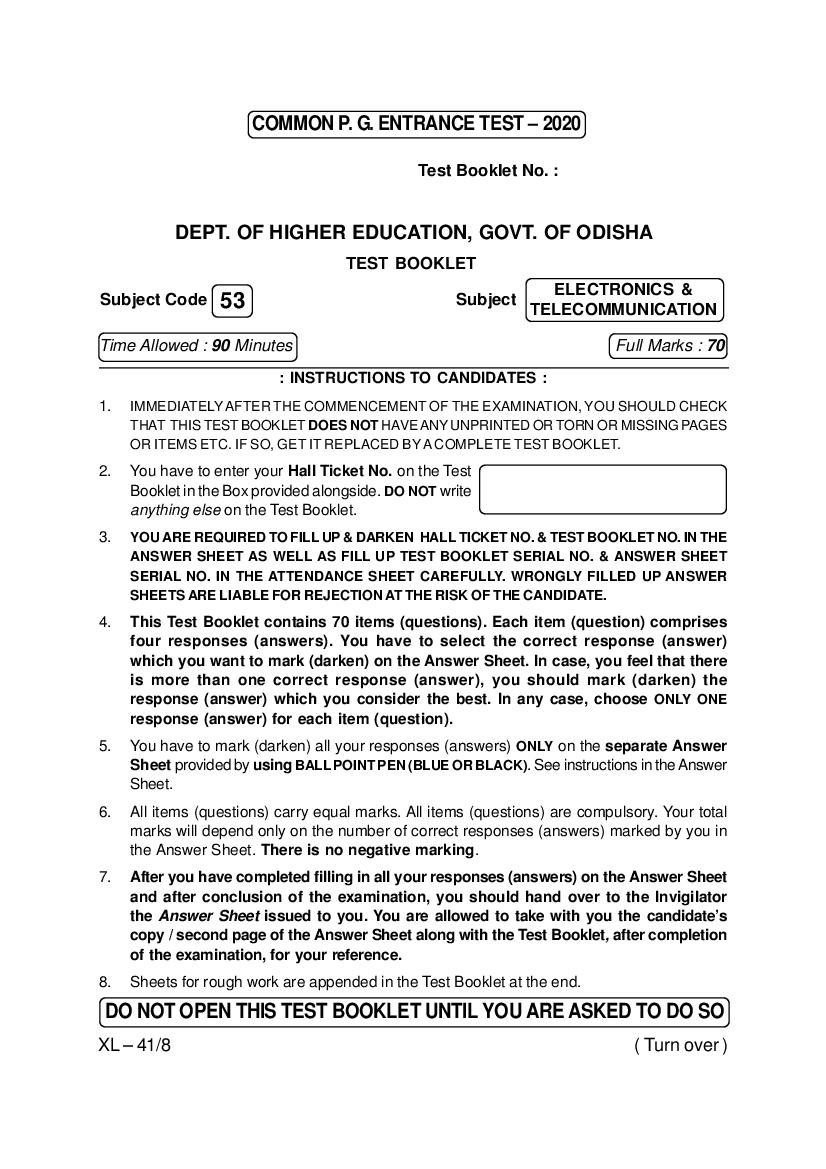
Test Booklet No. :
DEPT. OF HIGHER EDUCATION, GOVT. OF ODISHA
TEST BOOKLET
ELECTRONICS &
Subject Code 53 Subject
TELECOMMUNICATION
Time Allowed : 90 Minutes Full Marks : 70
: INSTRUCTIONS TO CANDIDATES :
1. IMMEDIATELY AFTER THE COMMENCEMENT OF THE EXAMINATION, YOU SHOULD CHECK
THAT THIS TEST BOOKLET DOES NOT HAVE ANY UNPRINTED OR TORN OR MISSING PAGES
OR ITEMS ETC. IF SO, GET IT REPLACED BY A COMPLETE TEST BOOKLET.
2. You have to enter your Hall Ticket No. on the Test
Booklet in the Box provided alongside. DO NOT write
anything else on the Test Booklet.
3. YOU ARE REQUIRED TO FILL UP & DARKEN HALL TICKET NO. & TEST BOOKLET NO. IN THE
ANSWER SHEET AS WELL AS FILL UP TEST BOOKLET SERIAL NO. & ANSWER SHEET
SERIAL NO. IN THE ATTENDANCE SHEET CAREFULLY. WRONGLY FILLED UP ANSWER
SHEETS ARE LIABLE FOR REJECTION AT THE RISK OF THE CANDIDATE.
4. This Test Booklet contains 70 items (questions). Each item (question) comprises
four responses (answers). You have to select the correct response (answer)
which you want to mark (darken) on the Answer Sheet. In case, you feel that there
is more than one correct response (answer), you should mark (darken) the
response (answer) which you consider the best. In any case, choose ONLY ONE
response (answer) for each item (question).
5. You have to mark (darken) all your responses (answers) ONLY on the separate Answer
Sheet provided by using BALL POINT PEN (BLUE OR BLACK). See instructions in the Answer
Sheet.
6. All items (questions) carry equal marks. All items (questions) are compulsory. Your total
marks will depend only on the number of correct responses (answers) marked by you in
the Answer Sheet. There is no negative marking.
7. After you have completed filling in all your responses (answers) on the Answer Sheet
and after conclusion of the examination, you should hand over to the Invigilator
the Answer Sheet issued to you. You are allowed to take with you the candidate’s
copy / second page of the Answer Sheet along with the Test Booklet, after completion
of the examination, for your reference.
8. Sheets for rough work are appended in the Test Booklet at the end.
DO NOT OPEN THIS TEST BOOKLET UNTIL YOU ARE ASKED TO DO SO
XL – 41/8 ( Turn over )
Page 2
Page 3
(A) 1,1
(B) –1, –1
(C) j, – j
(D) 1, –1
2. The trigonometric Fourier series of a periodic time function can have only :
(A) Cosine terms
(B) Sine terms
(C) Cosine and sine terms
(D) D.C. and cosine terms
3. If [f(t)] = F(s), then [f(t – T)] is equal to :
(A) esTF(s)
(B) e–sTF(s)
(C) F(s) / [1 – esT]
(D) F(s)/[1– e–sT]
4. The following differential equation has :
3d2y(t)/dt2 + 4(dy/dt)3 + y2 + 2 = x
(A) Degree = 2, order = 1
(B) Degree = 3, order = 2
(C) Degree = 4, order = 3
(D) Degree = 2,order = 3
5. A solution of the following differential equation is given by :
d2y/dx2 – 5dy/dx + 6y = 0
(A) y = e2x + e– 3x
(B) y = e2x + e3x
(C) y = e– 2x + e3x
(D) y = e– 2x + e– 3x
XL – 41/8 (3) ( Turn over )
Page 4
(A) 0 (B) 1
(C) 2 (D) 3
7. The minimum point of the function (x3/3) – x is at :
(A) x = 1 (B) x=–1
(C) x = 0 (D) x = 1/(3)1/2
8. The Laplace transform of sin(at) is :
(A) a/[s2 + a2] (B) s/[s2 + a2]
(C) a/[s2 – a2] (D) s/[s2 – a2]
9. A bag contains 8 white and 6 red balls. The probability of drawing two balls of the
same colour is :
(A) 21/91 (B) 13/112
(C) 43/91 (D) 41/91
10. The area enclosed between the parabola y = x2 and the straight line y = x is :
(A) 1/8 (B) 1/6
(C) 1/3 (D) 1/2
11. A square matrix A is Skew Hermitian if :
(A) Ao = A (B) AT= – A
(C) Ao= – A (D) AT= A
12. The system of equations :
3x + y – z = 2
x + 2y + z = 3
– x + y + 4z = 9
has a unique solution which is given by :
(A) x = 0, y = 1 and z = – 1 (B) x = 2, y = – 1 , z = 3
(C) x = 0, y = 0, z = 0 (D) x = 2, y = 0, z = 2
XL – 41/8 (4) ( Continued )
Page 5
(A) Circle
(B) Parabola
(C) Ellipse
(D) Pair of straight line
14. Inverse Laplace transform of s/[s2 + a2] is :
(A) (1/a) sin(at) (B) cos(at)
(C) (1/a) sinh(at) (D) cosh(at)
15. The product of two matrices A and adj.A is a :
(A) Zero matrix
(B) Unit matrix
(C) Scalar matrix
(D) Matrix A itself
16. If f(x) = | x | then :
(A) f(x) is continuous at x = 0
(B) f(x) is not continuous at x = 0
(C) f(x) is differentiable at x = 0
(D) None of these
17. The computer program which converts statements written in high level language to
object code is known as :
(A) Assembler
(B) Compiler
(C) Disassembler
(D) Operating system
18. The term AB + AC + BC reduce to :
(A) AB + CA (B) AC + BC
(C) AC + BC′ (D) AB + (BC)′
XL – 41/8 (5) ( Turn over )
Page 6
(A) 16 (B) 256
(C) 1024(1k) (D) 64k(64 x 1024)
20. Let A = [2 – 0.1 ; 0 3] and A–1= [1/2 a ; 0 b]. Then (a + b) = ?
(A) 7/20 (B) 3/20
(C) 19/60 (D) 11/20
21. In a forward biased photo diode with increase in incident light intensity, the diode
current :
(A) Increases
(B) Remains constant
(C) Decreases
(D) Remaining constant , the voltage drop across the diode increases
22. In a junction diode :
(A) The depletion capacitance decreases with increase in the reverse bias
(B) The diffusion capacitance increases with increase in the forward bias
(C) The diffusion capacitance is much higher than the depletion capacitance when
it is forward bias
(D) All of the above
23. Negative feedback in amplifiers :
(A) Improves the signal to noise ratio at the input
(B) Improves the signal to noise ratio at the output
(C) Reduces distortion
(D) Both (B) and (C)
24. Superposition theorem is not applicable to networks containing :
(A) Nonlinear elements
(B) Dependent voltage sources
(C) Dependent current sources
(D) Transformers
XL – 41/8 (6) ( Continued )
Page 7
(A) Is positively charged
(B) Is electrically neutral
(C) Has an electric field directed along its length
(D) Acts as a dipole
26. The electron and hole concentrations in an intrinsic semiconductor are ni and
prespectively. When doped with a p-type material, these change to n and p,
respectively. Then :
(A) n + p = ni+ pi (B) n + ni = p + pi
(C) npi = nip (D) np = nipi
27. In a differential amplifier, CMRR can be improved by using an increased :
(A) Emitter resistance
(B) Collector resistance
(C) Power supply voltages
(D) Source resistance
28. One input terminal of high gain comparator circuit is connected to ground and a
sinusoidal voltage is applied to the other input. The output of comparator will be :
(A) A sinusoid (B) A full rectified sinusoid
(C) A half rectified sinusoid (D) A square wave
29. An I/O processor control the flow of information between :
(A) Cache memory and I/O devices
(B) Main memory and I/O devices
(C) Two I/O devices
(D) Cache and main memories
30. An instruction used to set the Carry Flag in a microprocessor can be classified as :
(A) Data transfer (B) Arithmetic
(C) Logical (D) Program control
XL – 41/8 (7) ( Turn over )
Page 8
1101 is :
(A) 110100 (B) 001101
(C) 110111 (D) 111101
32. The early effect in a bipolar junction transistor is caused by :
(A) Fast turn on
(B) Fast turn off
(C) Large collector base reverse bias
(D) Large emitter base forward bias
33. The number of hardware interrupts (which require an external signal to interrupt)
present in an 8085 microprocessor are :
(A) 1 (B) 4
(C) 5 (D) 13
34. The MOSFET can be used as :
(A) Current controlled capacitor
(B) Voltage controlled capacitor
(C) Current controlled inductor
(D) Voltage controlled inductor
35. The ideal OPAMP has the following characteristics :
(A) Ri= ∞ , A = ∞, R0= 0
(B) Ri= 0, A = ∞, R0= 0
(C) Ri= ∞, A = ∞, R0= ∞
(D) Ri= 0, A = ∞, R0= ∞
36. The VSWR can have any value between :
(A) 0 and 1 (B) –1 and 1
(C) 0 and ∞ (D) 1 and ∞
XL – 41/8 (8) ( Continued )
Page 9
(A) Germanium (B) Aluminium
(C) Boron (D) Phosphorus
38. The input to a coherent detector is DSB - SC signal plus noise. The noise at the
detector output is :
(A) In phase component
(B) Quadrature component
(C) Zero
(D) Envelope
39. The noise at the input to an ideal frequency detector is white. The detector is operating
above threshold. The power spectral density of the noise at the output is :
(A) Raised cosine
(B) Flat
(C) Parabolic
(D) Gaussian
40. The cascode amplifier is a multistage configuration of :
(A) CC – CB (B) CE – CB
(C) CB – CC (D) CE – CC
41. Refractive index of glass is 1.5. Find the wavelength of a beam of light with a frequency
of 1014Hz in glass. Assume velocity of light is 3 x 10⁸ m/s in vacuum :
(A) 3µm
(B) 3mm
(C) 2µm
(D) 1µm
XL – 41/8 (9) ( Turn over )
Page 10
Group 1 Group 2
(a) Varactor diode (i) Voltage Reference
(b) PIN diode (ii) High frequency switch
(c) Zener diode (iii) Tuned circuits
(d) Schottky diode (iv) Current Controlled attenuator
(A) (a) – (iv), (b) – (ii), (c) – (i), (d) – (iii)
(B) (a) – (ii), (b) – (iv), (c) – (i), (d) – (iii)
(C) (a) – (iii), (b) – (iv), (c) – (i), (d) – (ii)
(D) (a) – (i), (b) – (iii), (c) – (ii), (d) – (iv)
43. The electric field lines and equipotential lines :
(A) Are parallel to each other
(B) Are one and the same
(C) Cut each other orthogonally
(D) Can be inclined to each other at any angle
44. The velocity of a travelling electromagnetic wave in free space is given by :
(A) µ0ε0
(B) (µ0ε0)1/2
(C) 1/(µ0ε0)1/2
(D) 1/(µ0ε0)
45. Which of the following statements is true ?
(A) ROM is a Read/Write memory.
(B) PC points to the last instruction that was executed.
(C) Stack works on the principle of LIFO.
(D) All instructions affect the flags.
XL – 41/8 ( 10 ) ( Continued )
Page 11
(A) Single frequency component
(B) Continuous frequency spectrum
(C) Spectrum of even harmonics
(D) Spectrum of odd harmonics
47. A Zener diode works on the principle of :
(A) Tunnelling of charge carriers across the junction
(B) Thermionic emission
(C) Diffusion of charge carriers across the junction
(D) Hoping of charge carriers across the junction.
48. The spectral density of pink noise varies as :
(A) 1/f2 (B) f2
(C) 1/f (D) f
49. Which memory does not require programming equipment ?
(A) RAM (B) EPROM
(C) EEPROM (D) UVPROM
50. Frequencies in UHF range propagate by means of :
(A) Ground waves
(B) Sky waves
(C) Space waves
(D) Surface waves
51. The bandwidth of an RF tuned amplifier is dependent on :
(A) Q-factor of the tuned output circuit
(B) Q-factor of the tuned input circuit
(C) Quiescent operating point
(D) Q factors of the output and input circuits as well as the quiescent operating
point
XL – 41/8 ( 11 ) ( Turn over )
Page 12
has the dominant advantage of :
(A) Higher current carrying capacity
(B) Lower peak inverse voltage requirement
(C) Lower ripple factor
(D) Higher efficiency
53. The binary fraction 0.0111 in decimal form is equal to :
(A) 0.4375 (B) 0.6225
(C) 0.8325 (D) 0.1105
54. Which of the following represents the noise figure ?
(A) (Si/Ni)/(So/No) (B) (So/No)/(Si/Ni)
(C) (So/No)/(Si/Ni)1/2 (D) (Si/Ni)/(So/No)1/2
55. Bit is a unit of :
(A) Entropy (B) Information
(C) Channel capacity (D) Rate of information
56. Code used in teleprinter is :
(A) Morse code (B) Five unit code
(C) Five unit synchronous code (D) Five unit start stop code
57. Choose the correct match for input resistance of various amplifier configurations
shown below :
Configuration Input Resistance
CB : Common Base LO : LOW
CC : Common Collector MO : MODERATE
CE : Common Emitter HI : HIGH
(A) CB-LO, CC-MO, CE-HI
(B) CB-LO, CC-HI, CE-MO
(C) CB-MO, CC-HI, CE-LO
(D) CB-HI, CC-LO, CE-MO
XL – 41/8 ( 12 ) ( Continued )
Page 13
(A) RL = 1/GC (B) RL = GC
(C) LG = RC (D) RG = LC
59. A band limited signal is sampled at the Nyquist rate. The signal can be recovered by
passing the sample through :
(A) An RC filter
(B) An envelope detector
(C) A PLL
(D) An ideal low pass filter with the appropriate bandwidth
60. The number of independent loops for a network with n nodes and b branches is :
(A) n – 1
(B) b – n
(C) b – n + 1
(D) Independent of the number of nodes
61. Schottky clamping is restored in TTL gates :
(A) To reduce propagation delay
(B) To increase noise margins
(C) To increase packing density
(D) To increase fan-out
62. The Eber-Moll model is applicable to :
(A) BJT (B) NMOS Transistors
(C) UJT (D) JFET
63. An R-S latch is a :
(A) Combinational circuit (B) Synchronous sequential circuit
(C) One bit memory element (D) One clock delay element
64. A PLL can be used to demodulate :
(A) PAM signals (B) PCM signals
(C) FM signals (D) DSB-SC signals
XL – 41/8 ( 13 ) ( Turn over )
Page 14
(A) An ADC (B) An Integrator
(C) A band pass filter (D) A high pass filter
66. The minimum number of MOS transistors required to make a dynamic RAM Cell is :
(A) 1 (B) 2
(C) 3 (D) 4
67. When a CPU is interrupted, it :
(A) Stops execution of instructions
(B) Acknowledges interrupt and branches of subroutines
(C) Acknowledges interrupt and continues
(D) Acknowledges interrupt and waits for the next instructions from the interrupting
device
68. In a microprocessor, the register which holds the address of the next instruction to be
fetched is :
(A) Accumulator (B) Program counter
(C) Stack pointer (D) Instruction register
69. The built in potential (Diffusion Potential) in a p-n junction :
(A) Is equal to the difference in the fermi level of the two sides, expressed in volts
(B) Increases with the increase in the doping levels of the two sides
(C) Increases with the increase in temperature.
(D) All of the above
70. Flat top sampling of low pass signal :
(A) Gives rise to aperture effect
(B) Implies oversampling
(C) Leads to aliasing
(D) Introduces delay distortion
XL – 41/8 ( 14 ) ( Continued )
Page 15
XL – 41/8 (230) ( 15 ) Electronics & Telecommunication
Document Details
| Board / Org | Odisha Exams |
| Exam | Odisha CPET |
| Type | Question Paper |
| Pages | 15 |
| Updated | 22 Jul 2026 |