Karnataka 2nd PUC Model Question Paper 2027 for Electronics (Paper 5)
Finished viewing? Save it for later —
Download Karnataka 2nd PUC Model Question Paper 2027 for Electronics (Paper 5) (PDF · 4 pages)About Karnataka 2nd PUC Model Question Paper 2027 for Electronics (Paper 5)
Karnataka 2nd PUC Model Question Paper 2027 for Electronics (Paper 5) is available here for free download. Published by Karnataka Board for Class 12, this sample paper can be viewed online or downloaded as a PDF (4 pages). Candidates preparing for Class 12 can use Karnataka 2nd PUC Model Question Paper 2027 for Electronics (Paper 5) to understand the exam pattern, the type of questions asked, and the overall difficulty level.
Frequently Asked Questions
How can I download Karnataka 2nd PUC Model Question Paper 2027 for Electronics (Paper 5)?
Open this page and click the Download button to save Karnataka 2nd PUC Model Question Paper 2027 for Electronics (Paper 5) as a PDF. It is completely free on AglaSem Docs.
Is Karnataka 2nd PUC Model Question Paper 2027 for Electronics (Paper 5) free to download?
Yes. Karnataka 2nd PUC Model Question Paper 2027 for Electronics (Paper 5) can be viewed online and downloaded as a PDF free of cost on AglaSem Docs.
How many pages does Karnataka 2nd PUC Model Question Paper 2027 for Electronics (Paper 5) have?
Karnataka 2nd PUC Model Question Paper 2027 for Electronics (Paper 5) contains 4 pages, which you can read online or download together as a single PDF.
Where can I find more Class 12 study material?
You can find more Class 12 question papers, sample papers, syllabus, and answer keys on AglaSem Docs.
Karnataka 2nd PUC Model Question Paper 2027 for Electronics (Paper 5) – Text
Read the full text of this sample paper below — useful to quickly search, copy and reference the content online without downloading the PDF.
📄 View text version (5 pages)
Page 1
Karnataka 2nd PUC
Model Question Paper
2027 for Electronics
(Paper 5)
EXAM YEAR TYPE SUBJECT
Karnataka Class 12 2027 Sample Paper Electronics
Notes · Sample Papers · Previous Year Papers · Mock Tests
Page 2
.co s e m
s em l a
a ag
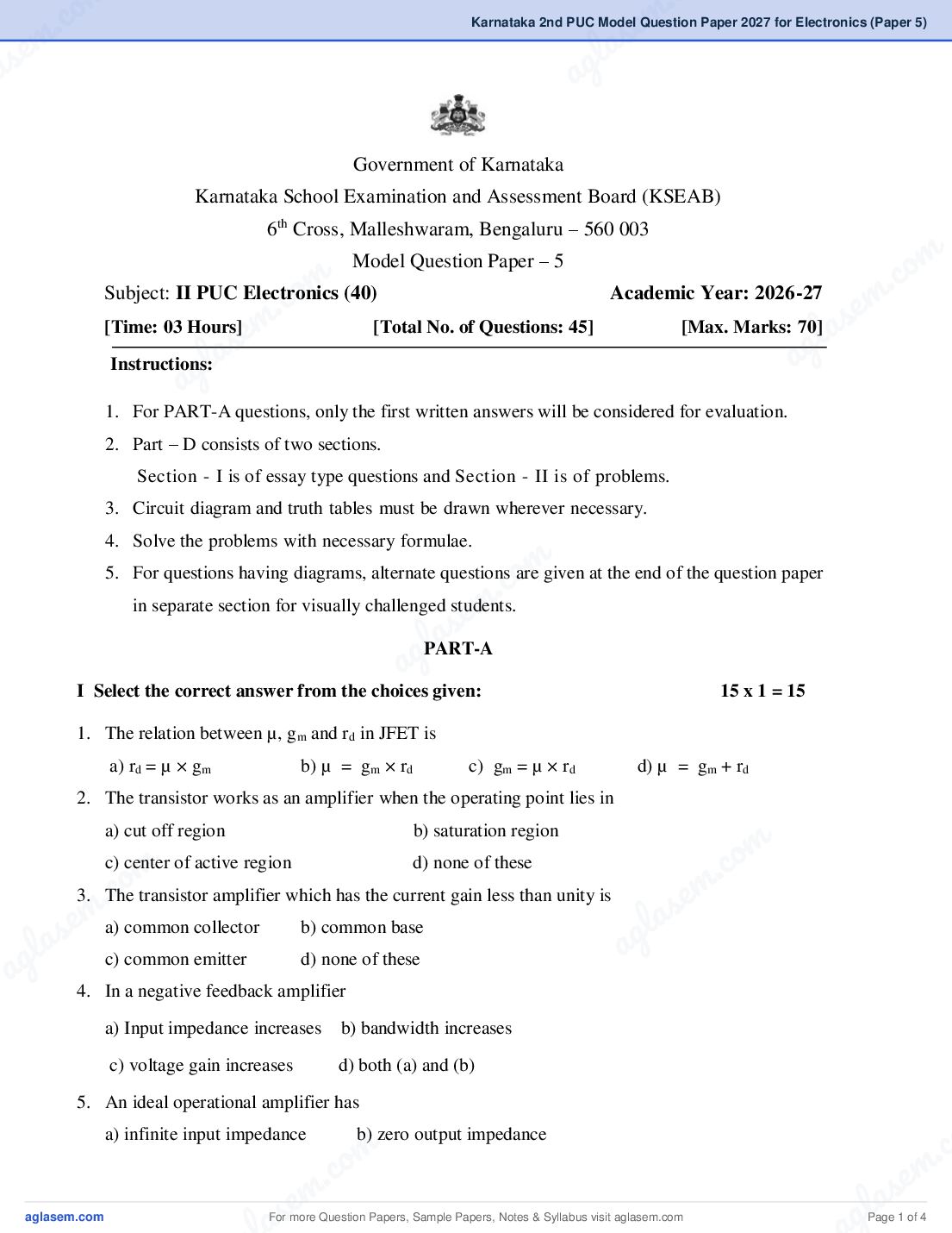
Government of Karnataka
Karnataka School Examination and Assessment Board (KSEAB)
6th Cross, Malleshwaram, Bengaluru – 560 003
Model Question Paper – 5
o m
m . c
. co (40)
Subject: II PUC Electronics Academic Year: 2026-27
s e m
[Time: 03 Hours] m [Max. Marks: 70] a
s e [Total No. of Questions: 45]
g l
Instructions:l
g a a
a
1. For PART-A questions, only the first written answers will be considered for evaluation.
2. Part – D consists of two sections.
Section - I is of essay type questions and Section - II is of problems.
3. Circuit diagram and truth tables must be drawn wherever necessary.
4. Solve the problems with necessary formulae.
o m
. c
5. For questions having diagrams, alternate questions are given at the end of the question paper
e m
in separate section for visually challenged students.
l as
ag
PART-A
I Select the correct answer from the choices given: 15 x 1 = 15
1. The relation between µ, gm and rd in JFET is
a) rd = µ × gm b) µ = gm × rd c) gm = µ × rd d) µ = gm + rd
2. The transistor works as an amplifier when the operating point lies in
m
a) cut off region b) saturation region
m
c) center of active region d) none of these
.co
.co
3. The transistor amplifier which has the current gain less than unity is
s e m
s ema) common collector b) common base g la
g la c) common emitter d) none of these a
a 4. In a negative feedback amplifier
a) Input impedance increases b) bandwidth increases
c) voltage gain increases d) both (a) and (b)
5. An ideal operational amplifier has
a) infinite input impedance
m
b) zero output impedance
. c
c. o s e m
s em
For more Question Papers, Sample Papers, Notes & Syllabus visit
gl a
Page 1 of 4
Page 3
6. A special case of non inverting amplifier in which all of the output voltage is feedback to the
inverting input of the op amp is called
a) differentiator b) integrator
c) logarithmic amplifier d) voltage follower
7. The crystal oscillator works on the principle of
a) Piezomagnetic effect b) Piezoelectric effect c) Both a and b d) None of these
8. The nearest ionospheric layer to the earth surface during day time is
a) D layer b) E layer c) F1 layer d) F2 layer
9. AM wave is distorted when
a) ma = 0 b) ma = 0.5 c) ma = 0.75 d) ma > 1.0
10. Identify the power device
a) SCR b) TRIAC c) MOSFET d) all of these
11. Sum of product equation can be realized by
a) XOR gates b) XNOR gates c) NOR-NOR gates d) NAND-NAND gates
12. BCD code for (23)10 is
a) 00010111 b) 01010110 c) 00100011 d) none of these
13. The data bits of Register A of 8051 is
a) 64 Bits b) 32 Bits c) 16 Bits d) 8 Bits
14. The operator ‘ &’ in C programming denotes
a) Bitwise OR b) Logical AND
c) Bitwise AND d) Exclusive OR
15. The abbreviation of MTSO is
a) Mobile Technology Switching Office b) Mobile Telephone System Office
c) Mobile Telephone Switching Office d) Mobile Technology System Office
II Fill in the blanks by choosing appropriate answer from the bracket: 5x1=5
[ a) amplifier b) amplitude c) damped d) universal e) zero f) encoder ]
16. The circuit which increases the strength of a weak signal is known as ………….
17. A zero crossing detector circuit switches its output state every time input signal crosses ……..
level.
18. Tank circuit produces …………… oscillations
2
For more Question Papers, Sample Papers, Notes & Syllabus visit Page 2 of 4
Page 4
.co s e m
s em g l a
a a
19. In frequency modulation ……………of the carrier remains same.
20. Logic gates used to realize other gates are known as …………… gates.
PART-B
III Answer any FIVE questions. 5 × 2 = 10
21. Mention any two types of transistor biasing circuits.
o m
o m . c
. c
22. In a negative feedback amplifier V = 20smV, V = 15 mV,
i V = 5 mV and
f V = 800 mV. Determine
o
e m
A, A and β.
e m l as
s
f
la
23. Determine the frequency of oscillation in a transistor Colpitt’s oscillator. Given L = 10 mH,
ag
C = 50 𝑛F.
eq a g
24. Write the expressions for amplitude and frequency of LSB in AM.
25. Draw the VI characteristics of power diode under forward biased condition for two temperatures.
26. Draw the logic circuit of a full adder using 3 input X-OR gate.
27. Write the features of 8051 microcontroller.
m
28. Distinguish between uplink and down link signals.
m
PART-C .co
s e
IV Answer any FIVE questions
l a 5 × 3 = 15
GS ag and hence on drain current I in JFET.
29. Explain the effect of V on depletion layer D
30. Derive an expression for input impedance of negative feedback amplifier.
31. Sketch nature of oscillator output waveforms for (a) Aβ > 1, (b) Aβ < 1 and (c) Aβ = 1
32. What is Line of Sight? Differentiate between radio horizon and optical horizon.
33. What are the characteristics of a good receiver?
34. Determine Vdc and Idc of SCR HWR. Given firing angle is 900 and rms voltage of ac input to
m
c o m
the rectifier is 230 V and load is 20 Ω.
m .co
. s e
emDraw the block diagram of a RADAR system. a
35. Convert the Boolean expression Y = AB + C into canonical SOP form.
s g l
la a
36.
ag PART-D (Section I)
V Answer any THREE questions. 3 × 5 = 15
37. With circuit diagram explain the working of CE amplifier.
38. Derive an expression for the output voltage of a summing amplifier.
39. Realize NOT, OR, AND and XNOR gates using NOR gates.
om
3
. c
. c e m
m as
se
For more Question Papers, Sample Papers, Notes & Syllabus visit
gl
Page 3 of 4
Page 5
save the result in register R0. What is the content of R0 after execution of the program?
41. Write a C program to accept two integer number and print whether they are equal or not equal.
PART-D (Section II)
VI Answer any TWO questions. 2 × 5 = 10
42. Find the input impedance, output impedance and voltage gain of the CE transistor amplifier for
the data given below: R1 = 47 kΩ, R2 = 12 kΩ, RC = 3.3 kΩ, RE = 1 kΩ,
RL = 10 kΩ, VCC = 18 V, β = 100, VBE = 0.7 V and re’ = 26mV/IE.
43. Calculate the output voltage Vo for the circuit shown below.
(3+2)
44. A 20 kW carrier wave is amplitude modulated at 70% depth of modulation by a sinusoidal
modulating signal. Calculate (a) Total Power (b) Side band power (c) Power in each sideband.
45. Simplify the Boolean expression Y(A, B, C, D) = Σm(4,5,7,9,11,12,13,15) + Σd(1,3,8)
using K-map. Draw the NAND gate equivalent circuit to realize the simplified expression.
PART-E
(For visually challenged students only)
43. (i) An op-amp noninverting amplifier circuit is given with Ri = 10 kΩ, Rf = 22 kΩ
and Vin = 80 µV. Determine the output voltage V01. 3
(ii) An op-amp inverting amplifier circuit is given with Ri = 33 kΩ, Rf = 220 kΩ
V1 = 100 mV. Determine the output voltage V02. 2
*****
4
For more Question Papers, Sample Papers, Notes & Syllabus visit Page 4 of 4
Document Details
| Board / Org | Karnataka Board |
| Exam | Class 12 |
| Type | Sample Paper |
| Pages | 4 |
| Language | english |
| Updated | 03 Nov 2026 |