CUSAT CAT 2018 Question Paper Electronics
Finished viewing? Save it for later —
Download CUSAT CAT 2018 Question Paper Electronics (PDF · 28 pages)About CUSAT CAT 2018 Question Paper Electronics
CUSAT CAT 2018 Question Paper Electronics is available here for free download. Published by Cochin University for CUSAT Common Admission Test, this question paper can be viewed online or downloaded as a PDF (28 pages). Candidates preparing for CUSAT Common Admission Test can use CUSAT CAT 2018 Question Paper Electronics to understand the exam pattern, the type of questions asked, and the overall difficulty level.
Frequently Asked Questions
How can I download CUSAT CAT 2018 Question Paper Electronics?
Open this page and click the Download button to save CUSAT CAT 2018 Question Paper Electronics as a PDF. It is completely free on AglaSem Docs.
Is CUSAT CAT 2018 Question Paper Electronics free to download?
Yes. CUSAT CAT 2018 Question Paper Electronics can be viewed online and downloaded as a PDF free of cost on AglaSem Docs.
How many pages does CUSAT CAT 2018 Question Paper Electronics have?
CUSAT CAT 2018 Question Paper Electronics contains 28 pages, which you can read online or download together as a single PDF.
Where can I find more CUSAT Common Admission Test study material?
You can find more CUSAT Common Admission Test question papers, sample papers, syllabus, and answer keys on AglaSem Docs.
CUSAT CAT 2018 Question Paper Electronics – Text
Read the full text of this question paper below — useful to quickly search, copy and reference the content online without downloading the PDF.
📄 View text version (28 pages)
Page 1
Subject Q Answer
Questions
Code Id Key
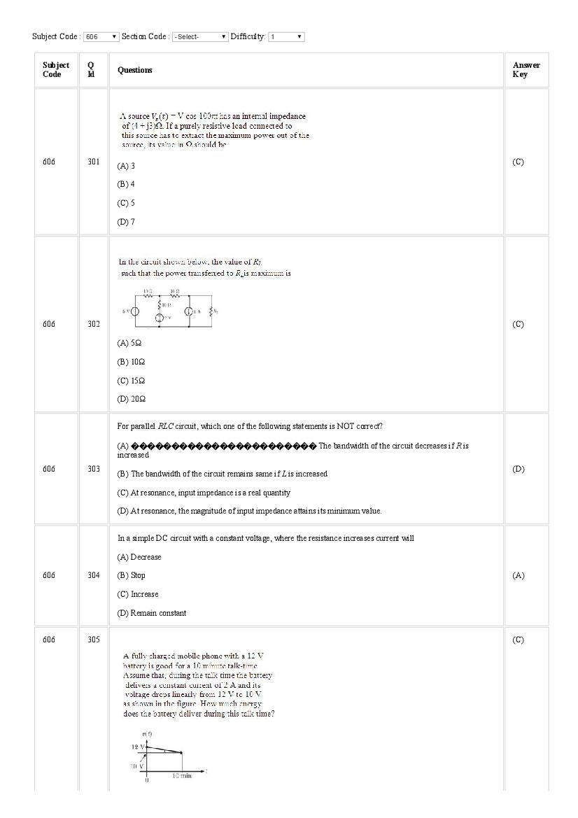
606 301 (C)
(A) 3
(B) 4
(C) 5
(D) 7
606 302 (C)
(A) 5Ω
(B) 10Ω
(C) 15Ω
(D) 20Ω
For parallel RLC circuit, which one of the following statements is NOT correct?
(A) ����������������������� The bandwidth of the circuit decreases if R is
increased
606 303 (D)
(B) The bandwidth of the circuit remains same if L is increased
(C) At resonance, input impedance is a real quantity
(D) At resonance, the magnitude of input impedance attains its minimum value.
In a simple DC circuit with a constant voltage, where the resistance increases current will
(A) Decrease
606 304 (B) Stop (A)
(C) Increase
(D) Remain constant
606 305 (C)
Page 2
(B) 12 kJ
(C) 13.2 kJ
(D) 14.4 J
(A)
606 306 (B) (D)
(C)
(D)
606 307 (A) (C)
(B)
(C)
(D)
(A)
606 308 (B) (C)
(C)
(D)
606 309 (B)
Page 3
(B)
(C)
(D)
(A)
606 310 (B) (A)
(C)
(D)
606 311 (A)
(A) delivers 80 W
(B) absorbs 80 W
(C) delivers 40 W
(D) absorbs 40 W
606 312 (A)
(A) ‒1/2
Page 4
(C) ‒3/2
(D) +3/2
Superposition theorem is NOT applicable to networks containing
(A) nonlinear elements
606 313 (B) dependent voltage sources (A)
(C) dependent current sources
(D) transformers
A high-Q quartz crystal exhibits series resonance at the frequency w s and parallel resonance at the frequency w p.
Then
(A) w sis very close to, but less than w p
606 314 (B) w s<< w p (A)
(C) w sis very close to, but greater than w p
(D) w s>> w p
The number of independent loops for a network with n nodes and b branches is
(A) n ‒1
606 315 (B) b ‒ n (C)
(C) b ‒ n +1
(D) independent of the number of nodes
In a forward biased pn junction diode, the sequence of events that best describes the mechanism of current flow is
(A) injection, and subsequent diffusion and recombination of minority carriers
606 316 (B) injection, and subsequent drift and generation of minority carriers (A)
(C) extraction, and subsequent diffusion and generation of minority carriers
(D) extraction, and subsequent drift and recombination of minority carriers
In a MOSFET operating in the saturation region, the channel length modulation effect causes
(A) an increase in the gate-source capacitance
606 317 (B) a decrease in the transconductance (D)
(C) a decrease in the unity-gain cutoff frequency
(D) a decrease in the output resistance
Thin gate oxide in a CMOS process is preferably grown using
(A) wet oxidation
606 318 (B) dry oxidation (B)
(C) epitaxial oxidation
(D) ion implantation
606 319 The DC current gain (β) of a BJT is 50. Assuming that the emitter injection efficiency is 0.995, the base transport (B)
factor is
(A) 0.98
(B) 0.985
Page 5
(D) 0.995
The phenomenon known as “Early Effect” in a bipolar transistor refers to a reduction of the effective base-width
caused by
(A) Electron - hole recombination at the base
606 320 (B)
(B) The reverse biasing of the base - collector junction
(C) The forward biasing of emitter-base junction
(D) The early removal of stored base charge during saturation-to-cut off switching
A MOS capacitor made using ‘p’ type substrate is in the accumulation mode. The dominan charge in the channel
is due to the presence of
(A) holes
606 321 (B)
(B) electrons
(C) positively charged icons
(D) negatively charged ions
606 322 (A)
(A) 106 Ohm
(B) 104 Ohm
(C) 10‒1 Ohm
(D) 10‒4 Ohm
606 323 (A) 2.26 eV (A)
(B) 1.98 eV
(C) 1.17 Ev
(D) 0.74 eV
The static characteristic of an adequately forward biased p- n junction is a straight line, if the plot is of
(A) log I vs log V
606 324 (B) log I vs V (B)
(C) I vs log V
(D) I vs V
In a bipolar transistor at room temperature, if the emitter current is doubled the voltage across its base-emitter
junction
(A) doubles
606 325 (C)
(B) halves
(C) increases by about 20 mV
(D) decreases by about 20 mV
Page 6
(A) is a monotonically increasing function of the collector current I C
(B) is a monotonically decreasing function of I C
(C) ����������������������� increase with I C , for low I C , reaches a maximum
and then decreases with further increase in IC
(D) is not a function of I C
For a MOS capacitor fabricated on a p-type semiconductor, strong inversion occurs when
(A) surface potential is equal to Fermi potential
(B) surface potential is zero
606 327 (D)
(C) ����������������������� surface potential is negative and equal to Fermi
potential in magnitude
(D) surface potential is positive and equal to twice the Fermi potential
606 328 (A) 0.25 (B)
(B) 0.5
(C) 0.75
(D) 1.0
(A)
606 329 (D)
(B)
(C)
(D)
Choose proper substitutes for X and Y to make the following statement correct Tunnel diode and Avalanche
photo diode are operated in X bias ad Y bias respectively.
(A) X: reverse, Y: reverse
606 330 (C)
(B) X: reverse, Y: forward
(C) X: forward, Y: reverse
(D) X: forward, Y: forward
606 331 (D)
Page 7
(B) 9.3 mA
(C) 6.67 mA
(D) 6.2 mA
606 332 (D)
(A) low pass filter
(B) band pass filter
(C) band stop filter
(D) high pass filter
606 333 (A)
(A) Only the frequency
(B) Only the amplitude
(C) Both the amplitude and the frequency
(D) Neither the amplitude nor the frequency
606 334 (D)
Page 8
(B) Positive feedback, V = 0 V
(C) Negative feedback, V = 5 V
(D) Negative feedback, V = 2 V
606 335 (B)
(A) high pass filter
(B) low pass filter
(C) band pass filter
(D) band reject filter
In a transconductance amplifier, it is desirable to have
(A) a large input resistance and a large output resistance
606 336 (B) a large input resistance and a small output resistance (A)
(C) aa small input resistance and a large output resistance
(D) a small input resistance and a small output resistance
606 337 (B)
(A) cut-off
(B) saturation
(C) normal active
(D) reverse active
606 338 (C)
Page 9
(B) Bias current of inverting and non-inverting input only
(C) Input offset current only
(D) Both the bias currents and input offset current
606 339 (D)
(A) 1 V
(B) 2 V
(C) 3 V
(D) 4 V
Voltage series feedback (also called series-shunt feedback) results in
(A) increase in both input and output impedances
606 340 (B) decrease in both input and output impedances (C)
(C) increase in input impedance and decrease in output impedance
(D) decrease in input impedance and increase in output impedance
606 341 (D)
(A) bridge rectifier
(B) ring modulator
(C) frequency discriminator
(D) voltage doubler
606 342 If the differential voltage gain and the common mode voltage gain of a differential amplifier are 48 dB and 2 dB (C)
Page 10
(A) 23 dB
(B) 25 dB
(C) 46 dB
(D) 50 dB
Generally, the gain of a transistor amplifier falls at high frequencies due to the
(A) internal capacitances of the device
606 343 (B) coupling capacitor at the input (B)
(C) skin effect
(D) coupling capacitor at the output
Three identical amplifiers with each one having a voltage gain of 50, input resistance of 1kΩ and output
resistance of 250Ω are cascaded. The opened circuit voltages gain of the combined amplifier is
(A) 49 dB
606 344 (C)
(B) 51 dB
(C) 98 dB
(D) 102 dB
606 345 (A)
(A) square wave
(B) triangular wave
(C) parabolic wave
(D) sine wave
606 346 (C)
(A) 0 V
(B) 5 mV
(C) + 15 V or ‒15 V
(D) +50 V or ‒ 50 V
606 347 A dc power supply has a no-load voltage of 30 V, and a full-load voltage of 25 V at a full-load current of 1 A. Its (B)
output resistance and load regulation, respectively, are
(A) 5 Ω and 20%
Page 11
(C) 5 Ω and 16.7%
(D) 25 Ω and 16.7%
For full wave rectification, a four diode bridge rectifier is claimed to have the following advantages over a two
diode circuit (1) less expensive transformer, (2) smaller size transformer, and (3) suitability for higher voltage
application. Of these,
(A) only (1) and (2) are true
606 348 (D)
(B) only (1) and (3) are true
(C) only (2) and (3) are true
(D) (1), (2) as well as (3) are true
606 349 (C)
(A) 0 mA,180 mA
(B) 5 mA,110 mA
(C) 10 mA, 55 mA
(D) 60 mA,180 mA
For small signal ac operation, a practical forward biased diode can be modelled as
(A) a resistance and a capacitance in series
606 350 (B) an ideal diode and resistance in parallel (C)
(C) a resistance and an ideal diode in series
(D) a resistance
The output Y of a 2-bit comparator is logic 1 whenever the 2-bit input A is greater than the 2-bit input B. The
number of combinations for which the output is logic 1, is
(A) 4
606 351 (B)
(B) 6
(C) 8
(D) 10
The full form of the abbreviations TTL and CMOS in reference to logic families are
(A) Triple Transistor Logic and Chip Metal Oxide Semiconductor
606 352 (B) Tristate Transistor Logic and Chip Metal Oxide Semiconductor (C)
(C) Transistor Transistor Logic and Complementary Metal Oxide Semiconductor
(D) Tristate Transistor Logic and Complementary Metal Oxide Silicon
606 353 What are the minimum number of 2- to -1 multiplexers required to generate a 2- input AND Gate and a 2-input (A)
Ex-OR gate
(A) 1 and 2
Page 12
(C) 1 and 1
(D) 2 and 2
X = 01110 and Y = 11001 are two 5-bit binary numbers represented in two’s complement format. The sum of X
and Y represented in two’s complement format using 6 bits is
(A) 100111
606 354 (C)
(B) 10000
(C) 101001
(D) correction in key
Decimal 43 in Hexadecimal and BCD number system is respectively
(A) B2, 0100 011
606 355 (B) 2B, 0100 0011 (B)
(C) 2B, 0011 0100
(D) B2, 0100 0100
A digital system is required to amplify a binary-encoded audio signal. The user should be able to control the gain
of the amplifier from minimum to a maximum in 100 increments. The minimum number of bits required to
encode, in straight binary, is
(A) 8
606 356 (D)
(B) 6
(C) 5
(D) 7
The minimum number of comparators required to build an 8-bits flash ADC is
(A) 8
606 357 (B) 63 (C)
(C) 255
(D) 256
A 4 bit ripple counter and a bit synchronous counter are made using flip flops having a propagation delay of 10
ns each. If the worst case delay in the ripple counter and the synchronous counter be R and S respectively, then
(A) R = 10 ns, S = 40 ns
606 358 (B)
(B) R = 40 ns, S = 10 ns
(C) R = 10 ns, S = 30 ns
(D) R = 30 ns, S = 10 ns
4 - bit 2’s complement representation of a decimal number is 1000. The number is
(A) +8
606 359 (B) 0 (D)
(C) ‒7
(D) ‒8
606 360 An 8 bit successive approximation analog to digital communication has full scale reading of 2.55 V and its (B)
conversion time for an analog input of 1 V is 20 �s. The conversion time for a 2 V input will be
(A) 10 �s
Page 13
(C) 40 �s
(D) 50 �s
The resolution of a 4-bit counting ADC is 0.5 volts. For an analog input of 6.6 volts, the digital output of the
ADC will be
(A) 1011
606 361 (B)
(B) 1101
(C) 1100
(D) 1110
Two 2’s complement number having sign bits ‘x’ and ‘y’ are added and the sign bit of the result is z. Then, the
occurrence of overflow is indicated by the Boolean function
(A)
(B)
606 362 (D)
(C)
(D)
The advantage of using a dual slope ADC in a digital voltmeter is that
(A) its conversion time is small
606 363 (B) its accuracy is high (B)
(C) it gives output in BCD format
(D) it does not require a
A dynamic RAM cell which hold 5 V has to be refreshed every 20 m sec, so that the stored voltage does not fall
by more than 0.5 V. If the cell has a constant discharge current of 1 pA, the storage capacitance of the cell is
(A)
(B)
606 364 (D)
(C)
(D)
A memory system of size 26 K bytes is required to be designed using memory chips which have 12 address lines
and 4 data lines each. The number of such chips required to design the memory system is
(A) 2
606 365 (D)
(B) 4
(C) 8
(D) 13
606 366 A band-limited signal with a maximum frequency of 5 kHz is to be sampled. According to the sampling theorem, (A)
the sampling frequency which is not valid is
(A) 5 kHz
(B) 12 kHz
Page 14
(D) 20 kHz
(A) time-invariant and stable
606 367 (D)
(B) stable and not time-invariant
(C) time-invariant and not stable
(D) not time-invariant and not stable
(A) stable and causal
606 368 (B)
(B) causal but not stable
(C) stable but not causal
(D) unstable and non-causal
606 369 (A) ‒1 (C)
(B) 0
(C) 1
(D) ∞
(A) 40
606 370 (A)
(B) 41
(C) 42
(D) 82
The Fourier transform of a conjugate symmetric function is always
(A) imaginary
606 371 (B) conjugate anti-symmetric (C)
(C) real
(D) conjugate symmetric
606 372 (C)
(A) 0
(B) 1
(C) 2
Page 15
(A)
606 373 (B) (C)
(C)
(D)
(A) 1
606 374 (B)
(B) E/2
(C) 2E
(D) 4E
(A) a real and even function of ɷ
606 375 (A)
(B) a imaginary and odd function of ɷ
(C) an imaginary and even function of ɷ
(D) a real and odd function of ɷ
The return loss of a device is found to be 20 dB. The voltage standing wave ratio (VSWR) and magnitude of
reflection coefficient are respectively
(A) 1.22 and 0.1
606 376 (A)
(B) 0.81 and 0.1
(C) – 1.22 and 0.1
(D) 2.44 and 0.2
(A)
606 377 (B) (C)
(C)
(D)
606 378 (A)
Page 16
(B) 12.6 dB
(C) 11.5 dB
(D) 18 dB
A transmission line with a characteristic impedance of 100 Ω is used to match a 50 Ω section to a 200 Ω section.
If the matching is to be done both at 429MHz and 1GHz, the length of the transmission line can be approximately
(A) 82.5 cm
606 379 (C)
(B) 1.05m
(C) 1.58 cm
(D) 1.75m
A transmission line of characteristic impedance 50Ω is terminated by a 50Ω load. When excited by a sinusoidal
voltage source at 10 GHz, the phase difference between two points spaced 2 mm apart on the line is found to be
π/4 radians. The phase velocity of the wave along the line is
(A) 0.8 � 108m/s
606 380 (C)
(B) 1.2 � 108m/s
(C) 1.6 � 108m/s
(D) 3 � 108m/s
A transmission line has a characteristic impedance of 50 Ω and a resistance of 0.1 Ω /m. If the line is distortion
less, the attenuation constant (in Np/m) is
(A) 500
606 381 (D)
(B) 5
(C) 0.014
(D) 0.002
The electric field component of a time harmonic plane EM wave traveling in a nonmagnetic lossless dielectric
medium has an amplitude of 1 V/m. If the relative permittivity of the medium is 4, the magnitude of the time-
average power density vector (in W/m2) is
(A)
(B)
606 382 (C)
(C)
(D)
606 383 For a Hertz dipole antenna, the half power beam width (HPBW) in the E-plane is (C)
(A) 360o
(B) 180o
Page 17
(D) 45o
A uniform plane wave in the free space is normally incident on an infinitely thick dielectric slab (dielectric
constant Ԑ = 9). The magnitude of the reflection coefficient is
(A) 0
606 384 (C)
(B) 0.3
(C) 0.5
(D) 0.8
In the design of a single mode step index optical fibre close to upper cut-off, the single-mode operation is not
preserved if
(A) radius as well as operating wavelength are halved
606 385 (B)
(B) radius as well as operating wavelength are doubled
(C) radius is halved and operating wavelength is doubled
(D) radius is doubled and operating wavelength is halved
606 386 (A) Linearly polarized in the z–direction (C)
(B) Elliptically polarized
(C) Left-hand circularly polarized
(D) Right-hand circularly polarized
A transmission line is feeding 1 watt of power to a horn antenna having a gain of 10 dB. The antenna is matched
to the transmission line. The total power radiated by the horn antenna into the free space is
(A) 10 Watts
606 387 (A)
(B) 1 Watts
(C) 0.1 Watts
(D) 0.01 Watt
A rectangular wave guide having TE10 mode as dominant mode is having a cut off frequency 18 GHz for the
mode TE30. The inner broad-wall dimension of the rectangular wave guide is
(A) 5/3 cm
606 388 (C)
(B) 5 cm
(C) 5/2 cm
(D) 10cm
Refractive index of glass is 1.5. Find the wavelength of a beam of light with frequency of 1014 Hz in glass.
Assume velocity of light is 3 � 108 m/s in vacuum
(A) 3 �m
606 389 (C)
(B) 3 mm
(C) 2 �m
(D) 1 mm
606 390 Consider a lossless antenna with a directive gain of +6 dB. If 1 mW of power is fed to it the total power radiated (A)
Page 18
(A) 4 mW
(B) 1 mW
(C) 7 mW
(D) 1/4 mW
A plane electromagnetic wave propagating in freespace is incident normally on a large slab of loss-less, non-
magnetic, dielectric material with Ԑ > Ԑ0. Maxima and minima are observed when the electric field is measured
in front of the slab. The maximum electric field is found to be 5 times the minimum field. The intrinsic
impedance of the medium should be
(A) 120 πΩ
606 391 (D)
(B) 60 πΩ
(C) 600 πΩ
(D) 24 πΩ
The depth of penetration of electromagnetic wave in a medium having conductivity ‘σ’at a frequency of 1 MHz
is 25 cm. The depth of penetration at a frequency of 4 MHz will be
(A) 6.25 dm
606 392 (B)
(B) 12.50 cm
(C) 50.00 cm
(D) 100.00 cm
A uniform plane wave traveling in air is incident on the plane boundary between air and another dielectric
medium with Ԑ r= 4. The reflection coefficient for the normal incidence, is
(A) Zero
606 393 (D)
(B) 0.5 ∠180. 0
(C) 0.333 ∠0. 0
(D) 0.333 ∠180. 0
The VSWR can have any value between
(A) 0 and 1
606 394 (B) ‒1 and +1 (D)
(C) 0 and ∞
(D) 1 and ∞
A person with receiver is 5 Km away from the transmitter. What is the distance that this person must move
further to detect a 3-dB decrease in signal strength?
(A) 942 m
606 395 (B)
(B) 2070 m
(C) 4978 m
(D) 5320 m
606 396 (A)
(A) 45 MHz
(B) 90 MHz
Page 19
(D) 900 MHz
A uniform plane electromagnetic wave incident on a plane surface of a dielectric material is reflected with a
VSWR of 3. What is the percentage of incident power that is reflected?
(A) 0.1
606 397 (B)
(B) 0.25
(C) 0.5
(D) 0.75
The depth of penetration of wave in a lossy dielectric increases with increasing
(A) conductivity
606 398 (B) permeability (C)
(C) wavelength
(D) permittivity
606 399 (A) 15.9 �m (A)
(B) 20.9 �m
(C) 25.9 �m
(D) 30.9 �m
606 400 (A)
(A) 0
(B) 0.02 A
(C) ∞
(D) None of the above
(A)
606 401 (B) (C)
(C)
(D)
606 402 (B)
Page 20
(B)
(C)
(D)
If E denotes expectation, the variance of a random variable X is given by
(A) E [ X 2] - E 2 [ X]
606 403 (B) E [ X 2] + E 2 [ X] (A)
(C) E [ X2]
(D) E 2 [ X]
A zero-mean white Gaussian noise is passes through an ideal low pass filter of bandwidth 10 kHz. The output is
then uniformly sampled with sampling period ts = 0.03 msec. The samples so obtained would be
(A) correlated
606 404 (A)
(B) statistically independent
(C) uncorrelated
(D) orthogonal
A 1 mW video signal having a bandwidth of 100 MHz is transmitted to a receiver through cable that has 40 dB
loss. If the effective one-side noise spectral density at the receiver is 10–20 Watt/Hz, then the signal-to-noise ratio
at the receiver is
(A) 50 dB
606 405 (A)
(B) 30 dB
(C) 40 dB
(D) 60 dB
Two sinusoidal signals of same amplitude and frequencies 10 kHz and 10.1 kHz are added together. The
combined signal is given to an ideal frequency detector. The output of the detector is
(A) 0.1 kHz sinusoid
606 406 (A)
(B) 20.1 kHz sinusoid
(C) a linear function of time
(D) a constant
The noise at the input to an ideal frequency detector is white. The detector is operating above threshold. The
power spectral density of the noise at the output is
(A) raised-cosine
606 407 (C)
(B) flat
(C) parabolic
(D) Gaussian
Page 21
(A)
(B)
(C)
(D)
606 409 (A) 13.36 (C)
(B) 9.36
(C) 2.64
(D) 8
The line-of-sight communication requires the transmit and receive antennas to face each other. If the transmit
antenna is vertically polarized, for best reception the receiver antenna should be
(A) horizontally polarized
606 410 (B) vertically polarized (B)
(C) at 45o with respect to horizontal polarization
(D) at 45o with respect to vertical polarization
A band-limited signal with a maximum frequency of 5 kHz is to be sampled. According to the sampling theorem,
the sampling frequency, which is not valid, is
(A) 5 kHz
606 411 (A)
(B) 12 kHz
(C) 15 kHz
(D) 20 kHz
606 412 (A)
(A)
(B)
(C)
Page 22
The amplitude spectrum of a Gaussian pulse is
(A) uniform
606 413 (B) a sine function (C)
(C) Gaussian
(D) an impulse function
(A) volt
606 414 (B) volt-sec (A)
(C) volt/sec
(D)
The auto correlation function of an energy signal has
(A) no symmetry
606 415 (B) conjugate symmetry (D)
(C) odd symmetry
(D) even symmetry
(A)
606 416 (B) (A)
(C)
(D)
A fair dice is tossed two times. The probability that the second toss results in a value that is higher than the first
toss is
(A) 2/36
606 417 (D)
(B) 2/6
(C) 5/12
(D) �
606 418 (B)
(A) 1
(B) 2
Page 23
(D) 4
606 419 (A) a unique solution (B)
(B) no solution
(C) an infinite number of solutions
(D) exactly two distinct solutions
(A) 0.5
606 420 (C)
(B) 1
(C) 0.5a
(D) a
606 421 (C)
(A) 2.8 and 36
(B) 7 and 119
(C) 2.8 and 32
(D) 7 and 80
(A) 44.2W
606 422 (B)
(B) 50W
(C) 62.5W
(D) 125W
606 423 (B)
(A)
(B)
Page 24
(D)
The first and the last critical frequency of an RC -driving point impedance function must respectively be
(A) a zero and a pole
606 424 (B) a zero and a zero (C)
(C) a pole and a pole
(D) a pole and a zero
A source of angular frequency 1 rad/sec has a source impedance consisting of 1Ω resistance in series with 1 H
inductance. The load that will obtain the maximum power transfer is
(A) 1 Ω resistance
606 425 (C)
(B) 1 Ω resistance in parallel with 1 H inductance
(C) 1 Ω resistance in series with 1 F capacitor
(D) 1 Ω resistance in parallel with 1 F capacitor
A series RLC circuit has a resonance frequency of 1khz and a quality factor Q=100, If each of R,L and C is
doubled from its original value, the new Q of the circuit is
(A) 25
606 426 (B)
(B) 50
(C) 100
(D) 200
606 427 (A) non-reciprocal and passive (B)
(B) non-reciprocal and active
(C) reciprocal and passive
(D) reciprocal and active
In IC technology, dry oxidation (using dry oxygen) as compared to wet oxidation (using steam or water vapor)
produces
(A) superior quality oxide with a higher growth rate
606 428 (D)
(B) inferior quality oxide with a higher growth rate
(C) inferior quality oxide with a lower growth rate
(D) superior quality oxide with a lower growth rate
606 429 (D)
(A) 107
(B) 100
Page 25
(D) 0
Drift current in the semiconductors depends upon
(A) only the electric field
606 430 (B) only the carrier concentration gradient (C)
(C) both the electric field and the carrier concentration
(D) both the electric field and the carrier concentration gradient
A Zener diode, when used in voltage stabilization circuits, is biased in
(A) reverse bias region below the breakdown voltage
606 431 (B) reverse breakdown region (B)
(C) forward bias region
(D) forward bias constant current mode
A silicon PN junction is forward biased with a constant current at room temperature. When the temperature is
increased by 10�C, the forward bias voltage across the PN junction
(A) increases by 60 mV
606 432 (D)
(B) decreases by 60 mV
(C) increases by 25 mV
(D) decreases by 25 mV
At room temperature, a possible value for the mobility of electrons in the inversion layer of a silicon n-channel
MOSFET is
(A) 450 cm2 /V‒s
606 433 (A)
(B) 1350 cm2 /V‒s
(C) 1800 cm2 /V‒s
(D) 3600 cm2 /V‒s
Thin gate oxide in a CMOS process is preferably grown using
(A) wet oxidation
606 434 (B) dry oxidation (B)
(C) epitaxial oxidation
(D) ion implantation
606 435 (A) Reverse breakdown voltage is lower and depletion capacitance is lower (C)
(B) Reverse breakdown voltage is higher and depletion capacitance is lower
(C) Reverse breakdown voltage is lower and depletion capacitance is higher
(D) Reverse breakdown voltage is higher and depletion capacitance is higher
606 436 (C)
Page 26
(B) Holes
(C) Dopant atoms
(D) Valence electrons
The ratio of the mobility to the diffusion coefficient in a semiconductor has the units
(A) V‒1
606 437 (B) cm. V1 (A)
(C) V.cm‒1
(D) V. s
A silicon wafer has 100nm of oxide on it and is furnace at a temperature above 1000oC for further oxidation. The
oxidation rate
(A) is independent of current oxide thickness and temperature
606 438 (D)
(B) is independent of current oxide thickness but depends on temperature
(C) slows down as the oxide grows
(D) is zero as the existing oxide prevents further oxidation
The concentration of minority carriers in an extrinsic semiconductor under equilibrium is
(A) Directly proportional to doping concentration
606 439 (B) Inversely proportional to the doping concentration (A)
(C) Directly proportional to the intrinsic concentration
(D) Inversely proportional to the intrinsic concentration
606 440 (D)
(A) 5.0E-5
(B) 2000
(C) 10000
(D) 20000
606 441 (D)
(A) 0.98 mA
(B) 0.99 mA
(C) 1.0 mA
(D) 1.01 mA
606 442 For small increase in VG beyond 1V, which of the following gives the correct description of the region of (D)
Page 27
(A) Both the MOSFETs are in saturation region
(B) Both the MOSFETs are in triode region
(C) n-MOSFETs is in triode and p -MOSFET is in saturation region
(D) n- MOSFET is in saturation and p -MOSFET is in triode region
The input impedance ( Zi) and the output impedance ( Z0) of an ideal transconductance voltage controlled current
source amplifier are
(A) Zi= 0, Z0 = 0
606 443 (D)
(B) Zi= 0, Z0 = ∞
(C) Zi= ∞, Z0 = 0
(D) Zi= ∞, Z0 = ∞
(A)
606 444 (C)
(B)
(C)
(D)
If β DC is increased by 10%, the collector-to-emitter voltage drop
(A) increases by less than or equal to 10%
606 445 (B) decreases by less than or equal to 10% (B)
(C) increase by more than 10%
(D) decreases by more than 10%
In a full-wave rectifier using two ideal diodes, V dc and V m are the dc and peak values of the voltage respectively
across a resistive load. If PIV is the peak inverse voltage of the diode, then the appropriate relationships for this
rectifier are
(A)
606 446 (B) (B)
(C)
(D)
606 447 An amplifier without feedback has a voltage gain of 50, input resistance of 1 k Ω and output resistance of 2.5 kΩ. (A)
The input resistance of the current-shunt negative feedback amplifier using the above amplifier with a feedback
factor of 0.2, is
Page 28
(B)
(C)
(D)
Introducing a resistor in the emitter of a common amplifier stabilizes the dc operating point against variations in
(A) only the temperature
606 448 (B) only the β of the transistor (C)
(C) both temperature and β
(D) none of the above
Crossover distortion behavior is characteristic of
(A) Class A output stage
606 449 (B) Class B output stage (D)
(C) Class AB output stage
(D) Common-base output stage
In standing wave pattern on a transmission line
(A) voltage and current nodes coincide
606 450 (B) voltage nodes and current antinodes as well as current nodes and voltage antinodes coincide (D)
(C) voltage and current antinode coincide
(D) both (A) and (C)
Document Details
| Board / Org | Cochin University |
| Exam | CUSAT Common Admission Test |
| Type | Question Paper |
| Pages | 28 |
| Updated | 30 Apr 2026 |