Karnataka 2nd PUC Model Question Paper 2023 for Electronics
Finished viewing? Save it for later —
Download Karnataka 2nd PUC Model Question Paper 2023 for Electronics (PDF · 5 pages)About Karnataka 2nd PUC Model Question Paper 2023 for Electronics
Karnataka 2nd PUC Model Question Paper 2023 for Electronics is available here for free download. Published by Karnataka Board for Class 12, this sample paper can be viewed online or downloaded as a PDF (5 pages). Candidates preparing for Class 12 can use Karnataka 2nd PUC Model Question Paper 2023 for Electronics to understand the exam pattern, the type of questions asked, and the overall difficulty level.
Frequently Asked Questions
How can I download Karnataka 2nd PUC Model Question Paper 2023 for Electronics?
Open this page and click the Download button to save Karnataka 2nd PUC Model Question Paper 2023 for Electronics as a PDF. It is completely free on AglaSem Docs.
Is Karnataka 2nd PUC Model Question Paper 2023 for Electronics free to download?
Yes. Karnataka 2nd PUC Model Question Paper 2023 for Electronics can be viewed online and downloaded as a PDF free of cost on AglaSem Docs.
How many pages does Karnataka 2nd PUC Model Question Paper 2023 for Electronics have?
Karnataka 2nd PUC Model Question Paper 2023 for Electronics contains 5 pages, which you can read online or download together as a single PDF.
Where can I find more Class 12 study material?
You can find more Class 12 question papers, sample papers, syllabus, and answer keys on AglaSem Docs.
Karnataka 2nd PUC Model Question Paper 2023 for Electronics – Text
Read the full text of this sample paper below — useful to quickly search, copy and reference the content online without downloading the PDF.
📄 View text version (5 pages)
Page 1
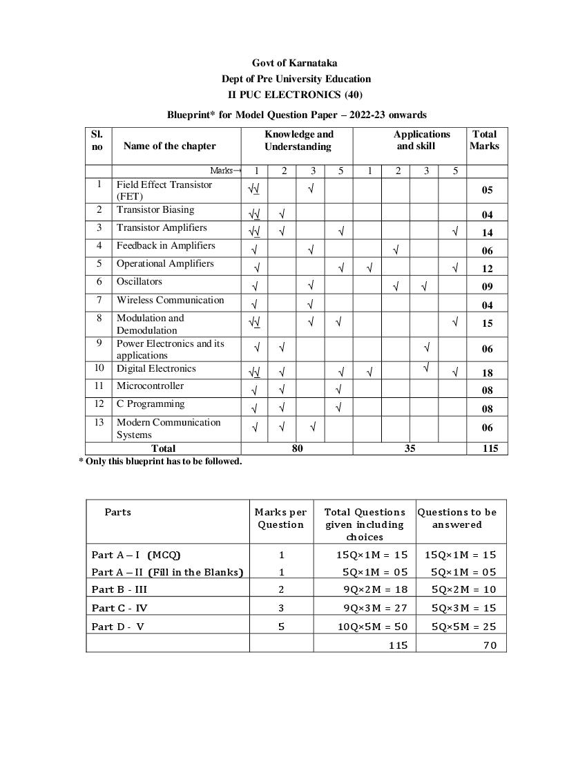
Dept of Pre University Education
II PUC ELECTRONICS (40)
Blueprint* for Model Question Paper – 2022-23 onwards
Sl. Knowledge and Applications Total
no Name of the chapter Understanding and skill Marks
Marks→ 1 2 3 5 1 2 3 5
1 Field Effect Transistor √√ √ 05
(FET)
2 Transistor Biasing
√√ √ 04
3 Transistor Amplifiers √√ √ √ √ 14
4 Feedback in Amplifiers √ √ √ 06
5 Operational Amplifiers
√ √ √ √ 12
6 Oscillators √
√ √ √ 09
7 Wireless Communication √ √ 04
8 Modulation and √√ √ √ √ 15
Demodulation
9 Power Electronics and its √ √ √ 06
applications
10 Digital Electronics √√ √ √ √ √ √ 18
11 Microcontroller √ √
√ 08
12 C Programming √ √
√ 08
13 Modern Communication √ √
√ 06
Systems
Total 80 35 115
* Only this blueprint has to be followed.
Parts Marks per Total Questions Questions to be
Question given including answered
choices
Part A – I (MCQ) 1 15Q×1M = 15 15Q×1M = 15
Part A – II (Fill in the Blanks) 1 5Q×1M = 05 5Q×1M = 05
Part B - III 2 9Q×2M = 18 5Q×2M = 10
Part C - IV 3 9Q×3M = 27 5Q×3M = 15
Part D - V 5 10Q×5M = 50 5Q×5M = 25
115 70
Page 2
MODEL QUESTION PAPER
Time: 3 Hour 15 min Max. Marks: 70
Instructions:
1. The question paper has four parts A, B, C and D.
2. Part - A is compulsory.
3. Part - D consists of essay type questions and problems together.
4. Circuit diagrams, timing diagrams and truth tables must be drawn wherever necessary.
5. Solve the problems with necessary formulas.
PART A
I. Select the correct answer from the choices given: 15 x 1 = 15
1. Name a unipolar device.
a) Diode b) BJT c) FET d) TRIAC
2. For faithful amplification the operating point is chosen at the
a) Centre of the active region b) Cut off region
c) Saturation region d) Inversion region
3. What is the phase difference between input and output of a transistor CB amplifier?
a) 00 b) 600 c) 900 d) 1800
4. What happens to the input impedance of an amplifier when voltage series negative
feedback is applied?
a) Remains same b) Increases
c) Decreases d) Oscillates
5. Virtual ground concept relates voltage at the inverting terminal VA to the voltage at non-
inverting terminal VB by the relation
a) VA > VB b) VA - VB = 0 c) VA < VB d) VA - VB = 1
6. Mention the output of an integrator if the sine wave is given to its input.
a) Cosine wave b) Sine wave
c) Square wave d) Triangular wave
7. Mention the high frequency stability oscillator
a) Crystal oscillator b) Hartley oscillator
c) Wein bridge oscillator d) Colpitts oscillator
Page 3
a) D layer b) E layer c) F1 layer d) F2 layer
9. How many sidebands present in AM?
a) 1 b) 2 c) 3 d) ∞
10. A SCR has
a) Two junctions and three layers b) Three junctions and three layers
c) Three junctions and four layers d) Four junctions and three layers
11. Gray code is used in shaft position
a) Multiplexer b) decoder c) encoder d) de-multiplexer
12. Logic expression for the output of XOR gate is
a) Y = ̅̅̅̅̅
AB b) Y = ̅̅̅̅̅̅̅
A+B ̅ B + AB
c) Y = A ̅ ̅B
d) Y = A ̅ + AB
13. How many timers are present in 8051 microcontroller?
a) 1 b) 2 c) 3 d) 4
14. Size of an integer in C programming is
a) 1 byte b) 2 byte c) 4 byte d) 8 byte
15. Shapes of cells in mobile network operation system is
a) Octagonal b) Circular c) Oval d) Hexagonal
II. Fill in the blanks by choosing appropriate answer from those given in the bracket: 5x1=5
[ a) data b) modulation c) biasing d) impedance e) switching speed ]
16. FET has high ……………….
17. Application of suitable voltage across the terminals of a transistor is called ……………
18. CC amplifier is used to match …………
19. Process of changing some characteristics of carrier in accordance with instantaneous value of
the signal is called ………
20. Flip-Flops are used to store ………...
PART B
III. Answer any FIVE questions: 5 x 2 = 10
21. Mention any two advantages of voltage divider biasing.
22. Write the steps involved in drawing DC equivalent circuit of an amplifier.
Page 4
feedback factor β = 0.1.
24. Determine frequency of Hartley oscillator. Given L1 = 4 mH, L2 = 2 mH and C =10 nf
25. Compare forward characteristics of power diode for two different junction
temperatures.
26. Write minterm designation table for two input variables.
27. Write any two comparisons between Microprocessor and Microcontroller.
28. Mention any four operators used in C programming.
29. Distinguish between uplink and downlink signals.
PART C
IV. Answer any FIVE questions: 5 x 3 = 15
30. Obtain the relations between FET parameters.
31. Give any three differences between positive feedback and negative feedback.
32. Draw the circuit diagram of phase shift oscillator. Write the expression for its frequency
of oscillations.
33. Determine frequency of tank circuit having L = 1 µH and C = 0.01 µF.
34. Draw the block diagram of basic communication system and explain the function of
each block.
35. Explain diode detector circuit.
36. Determine Vdc and Idc of SCR HWR. Given firing angle is 900 and rms voltage of ac input
to the rectifier is 230 V and load is 10 Ω.
37. What is half-adder? Draw the logic diagram of half adder using only NAND gates.
38. What is Internet? Mention the important techniques used for Bluetooth operation.
PART D
V. Answer any FIVE questions: 5 x 5 = 25
39. With a neat circuit diagram explain the working of two stage RC-coupled amplifier.
40. With the circuit diagram derive an expression for output voltage of three input op-amp
adder.
Page 5
42. Prove the universal properties of the NOR gate.
43. Write an assembly language program to add two numbers 1FH and B4H and store the result
in R0. Verify the result by binary addition.
44. Write a c-program to accept the three integers and print the largest amongst them.
45. Calculate the voltage gain, input impedance and output impedance in the circuit
given below. Given β = 100 and re’ =26mV/IE. .
46. Find the output voltage in the op-amp circuit given.
47. A 10 kW carrier wave is amplitude modulated at 80% depth of modulation by a sinusoidal
modulating signal. Calculate the total power and side band power of the AM wave.
48. Simplify the Boolean expression Y = Σm (1, 3, 5, 7, 13, 15) + Σd (0, 12, 14) using
K-map. Draw the NAND Gate equivalent circuit to realize the simplified equation.
*****
Document Details
| Board / Org | Karnataka Board |
| Exam | Class 12 |
| Type | Sample Paper |
| Pages | 5 |
| Updated | 30 Apr 2026 |