Karnataka 2nd PUC Question Paper 2026 Answer Key Electronics
Finished viewing? Save it for later —
Download Karnataka 2nd PUC Question Paper 2026 Answer Key Electronics (PDF · 7 pages)About Karnataka 2nd PUC Question Paper 2026 Answer Key Electronics
Karnataka 2nd PUC Question Paper 2026 Answer Key Electronics is available here for free download. Published by Karnataka Board for Class 12, this question paper can be viewed online or downloaded as a PDF (7 pages). Candidates preparing for Class 12 can use Karnataka 2nd PUC Question Paper 2026 Answer Key Electronics to understand the exam pattern, the type of questions asked, and the overall difficulty level.
Frequently Asked Questions
How can I download Karnataka 2nd PUC Question Paper 2026 Answer Key Electronics?
Open this page and click the Download button to save Karnataka 2nd PUC Question Paper 2026 Answer Key Electronics as a PDF. It is completely free on AglaSem Docs.
Is Karnataka 2nd PUC Question Paper 2026 Answer Key Electronics free to download?
Yes. Karnataka 2nd PUC Question Paper 2026 Answer Key Electronics can be viewed online and downloaded as a PDF free of cost on AglaSem Docs.
How many pages does Karnataka 2nd PUC Question Paper 2026 Answer Key Electronics have?
Karnataka 2nd PUC Question Paper 2026 Answer Key Electronics contains 7 pages, which you can read online or download together as a single PDF.
Where can I find more Class 12 study material?
You can find more Class 12 question papers, sample papers, syllabus, and answer keys on AglaSem Docs.
Karnataka 2nd PUC Question Paper 2026 Answer Key Electronics – Text
Read the full text of this question paper below — useful to quickly search, copy and reference the content online without downloading the PDF.
📄 View text version (7 pages)
Page 1
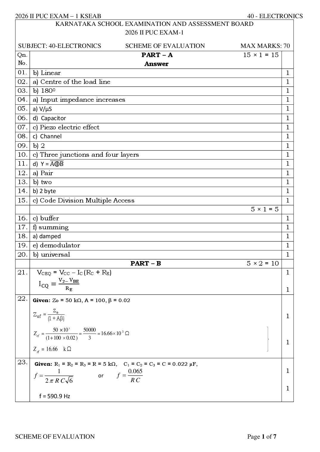
KARNATAKA SCHOOL EXAMINATION AND ASSESSMENT BOARD
2026 II PUC EXAM-1
SUBJECT: 40-ELECTRONICS SCHEME OF EVALUATION MAX MARKS: 70
Qn. PART – A 15 × 1 = 15
No. Answer
01. b) Linear 1
02. a) Centre of the load line 1
03. b) 1800 1
04. a) Input impedance increases 1
05. a) V/µS 1
06. d) Capacitor 1
07. c) Piezo electric effect 1
08. c) Channel 1
09. b) 2 1
10. c) Three junctions and four layers 1
11. d) Y = ̅̅̅̅̅̅̅
A⨁B 1
12. a) Pair 1
13. b) two 1
14. b) 2 byte 1
15. c) Code Division Multiple Access 1
5×1=5
16. c) buffer 1
17. f) summing 1
18. a) damped 1
19. e) demodulator 1
20. b) universal 1
PART – B 5 × 2 = 10
21. VCEQ = VCC – IC (RC + RE) 1
V2− VBE
ICQ =
RE 1
22. Given: Zo = 50 kΩ, A = 100, β = 0.02
Zo
Z of = 1
(1 + Aβ)
50 ×10 3 50000
Z of = = = 16.66 10 3
(1 + 100 0.02 ) 3
1
Z of = 16.66 k
23. Given: R1 = R2 = R3 = R = 5 kΩ, C1 = C2 = C3 = C = 0.022 µF,
1 0.065 1
f = or f =
2 R C 6 RC
1
f = 590.9 Hz
SCHEME OF EVALUATION Page 1 of 7
Page 2
or
𝑚𝑎 𝑉𝑐 𝑚𝑎 𝑉𝑐 1
vAM = Vc sinct + cos(c-m)t - cos(c+m)t
2 2
𝑉𝑚𝑎𝑥 −𝑉𝑚𝑖𝑛
ma =
𝑉𝑚𝑎𝑥 +𝑉𝑚𝑖𝑛 1
25. 1. Power diode
2. Power BJT
3. SCR
4. TRIAC
5. Power MOSFET
6. IGBT (Any four) 2
26. Full adder using 3-input XOR gate
2
27. (a) Internal RAM – 128 bytes 1
(b) Internal ROM – 4 k Bytes 1
28. Uplink Signal Downlink Signal
The signal transmitted from ground The signal transmitted from satellite to
station to satellite is called Uplink ground station is called Downlink
2
Transmitted signal is 6 GHz Transmitted signal is 4 GHz
PART – C 5 × 3 = 15
29. a) Drain resistance (rd) is the ratio of small change in drain-to-source
voltage (VDS) to the corresponding change in ID when gate-to-source
voltage (VGS) is constant.
or
∆V 1
rd = ∆IDS , when VGS is constant
D
b) Transconductance (gm) is the ratio of small change in drain current (ID)
to the corresponding change in gate-to-source voltage (VGS) when drain-
source-voltage is constant.
or 1
∆ID
g m = ∆V , when VDS is constant
GS
c) Amplification factor (μ) is the ratio of small change in VDS to the
corresponding change in VGS for a constant drain current ID.
or
∆V 1
µ = ∆VDS , when ID is constant
GS
SCHEME OF EVALUATION Page 2 of 7
Page 3
1
Let Vs be the input to the amplifier, Vi be the input to the basic amplifier, Vf be
the feedback voltage and Vo be the output voltage of the amplifier.
The open loop gain of amplifier is
Vo Vo = AVi …..(1)
A=
Vi
The closed loop gain of amplifier is
Vo
Af = ….. (2)
Vs
Feedback factor of voltage series negative feedback is
V Vf = βVo …..(3)
β= f
Vo
With negative feedback the input to the basic amplifier is
Vi = Vs – Vf
Vi = Vs – βVo [Since Vf = βVo from equation (3)] 2
Vi = Vs – βAVi [Since V0 = AVi from equation (1)]
Vs = Vi + AβVi
Vs = Vi(1+Aβ) ..…(4)
Substitute equation (4) in equation (2), we get
Vo
Af =
Vi (1 + Aβ)
A Vo
Af = [Since A = from equation (1)]
(1 + Aβ) Vi
31.
1
Aβ > 1
Aβ < 1 1
Aβ = 1
1
SCHEME OF EVALUATION Page 3 of 7
Page 4
ionospheric propagation that gets returned to the Earth. 1
Critical Frequency (fc) : It is the highest frequency of the beamed radio wave that
will be returned to the earth. 1
Skip Distance (∆) : It is the minimum distance between transmitting
antenna and first receiving antenna measured along the surface of the earth. 1
33. a) Sensitivity
b) Selectivity
c) Fidelity
d) Signal to noise ratio
e) Stability (Any three) 3
34. Given: Given: 𝛼 = 00, Vrms = 230 V, R = 10 Ω.
𝑉 1
Vdc = 𝜋𝑚 [1 + 𝑐𝑜𝑠𝛼] and Vm = Vrms√2 = 325.26 V,
∴
𝑉
Vdc = 𝜋𝑚 [1 + 1] = 207 V 1
𝑉𝑑𝑐
Idc = = 20.7 A 1
𝑅
35. Y = A + CB
Y = A( B + B )(C + C ) + ( A + A) BC
Y = ABC + ABC + A BC + A BC + ABC + ABC
3
Y = ABC + ABC + A BC + A BC + ABC
36. RADAR is an acronym for RAdio Detection And Ranging. It is a system used
for detecting or finding the exact location or determining the velocity of a 1
distant object. They are able to operate day and night, in all weathers, have
very broad coverage, and have high resolution imaging.
Applications of Radar:
1. Radars are used in defense weapons systems.
2. Safety navigational applications.
3. To find location of enemy missiles, planes and ships.
4. To Landing planes in bad weather conditions.
5. Used as altimeters to measure height. (Any two)
2
PART – D (Section I) 3 × 5 = 15
37.
2
1
1. VCC, VEE, RE, and RC provide the necessary DC bias to the transistor.
2. C1 and C2 are called the coupling capacitors whose function is to block the DC and
allow ac signals.
SCHEME OF EVALUATION Page 4 of 7
Page 5
By applying KVL to the output we get
vo = vcb = VCC - iC RC.
During positive half cycle of the input signal,
1. The forward bias between base and emitter junction decreases.
2. Consequently input current iE and collector current iC decreases.
3. Thus voltage drops across RC i.e. iCRC is decreased.
4. Hence output voltage vcb is increased. 1
Therefore we get positive half cycle at the output.
During negative half cycle of the input signal,
1. The forward bias between base and emitter junction increases.
2. Consequently input current iE and collector current IC increases.
3. Thus voltage drops across RC i.e. iCRC is increased.
4. Hence output voltage vcb is decreased 1
Therefore we get negative half cycle at the output.
Thus there is no phase reversal between input and output signals.
38. An amplifier whose output is in phase with the input is called the non-inverting
amplifier. 1
The circuit diagram of non-inverting op-amp is as shown.
For an ideal op-amp, open loop gain A = ∞ and input impedance, Zi = ∞
V
𝐴 = V −oV = ∞
B A
VB-VA = 0 or, VB = VA = Vi
Since input impedance Zi = ∞ Because ib = 0
2
Applying KCL at (A),
ii = ib + if
ii = if (since ib = 0)
(0 − VA ) (VA − Vo )
=
Ri Rf
2
Since VA = Vi,
(− Vi ) (Vi − Vo )
=
Ri Rf
Vo V V
→ = Ri + Ri
Rf f i
V V R R
Rf
Vo = R f (Ri + Ri ) Vo = Vi (Rf + Rf ) V0 = Vi( 1+ )
f i f i Ri
SCHEME OF EVALUATION Page 5 of 7
Page 6
out conditions are desirable in many applications.
However, the condition S = R = 1 generating an output Q = 𝑄̅ = 1 i.e. the invalid state
is undesirable. To avoid this condition a NOT gate between S and R inputs is placed. 1
This result as an SR flip flop is converted into DATA or D flip-flop. Here the data is fed
at the D input. The output Q simply follow the input D.
2
Logic circuit of D flip flop Logic symbol
Working of D flip flop
CLK D Qn+1 ̅̅̅̅̅̅̅
Qn+1 Comment
0 X Qn ̅̅̅̅
Qn HOLD
1 0 0 1 RESET
1 1 1 0 SET 2
a) When CLK = 0, D = X then the output is in HOLD (No change) state.
b) When CLK = 1, D = 0 then the output is at RESET state.
c) When CLK = 1, D = 1 then the output is at SET state.
40. Multiply 43H by 2AH
MOV A, #43H ; load 43H to reg.A
MOV B, #2AH ; load 2AH to reg.B
MUL AB ; 43H × 2AH
MOV R0, A ; Store Lower byte of the product in R0
MOV R1, B ; Store Higher byte of the product in R1 5
41. #include <stdio.h>
void main()
{
float radius, area;
printf(“Enter the value of radius\n”);
scanf(“%f”, &radius);
area = 3.142*radius*radius;
printf(“Area of the circle = %f”, area);
5
}
PART D (Section II) 2 x 5 = 10
42. Given: β = 100, R1 = 90 kΩ, R2 = 22 kΩ, RC = 5 kΩ, RE = 1 kΩ, VCC =12 V
V
(a) V2 = R1+R2
cc
× R2
12
V2 = 90K+22K × 22 k
SCHEME OF EVALUATION Page 6 of 7
Page 7
V −V
(b) IE = 2 R BE
E
2.35−0.7 1
IE = = 1.65 mA
1𝑘
26 mV 26 mV
(c) re1 = = 1.65 𝑚𝐴 = 15.75 Ω 1
IE
Rc 5k
(d) Av = r = 15.75Ω = 317 1
e′
(e) zin(base) = βre1 = 100 x 15.75
= 1.575 kΩ 1
43. (a) Given circuit is a subtractor circuit. Given V1 = 1 V, V2 = 2 V.
Since Rf = R3 and R1 = R2
R
The output of subtrator is Vo1 = R f (V2 –V1)
50 𝑘
1
3
Vo1 = (2 –1) = 5 V
10 𝑘
(b) Given circuit is a inverting amplifier
Output of inverting amplifier is given by
Rf
Vo2 = - Vin
Ri
20k 2
Vo2 = - 3 =-6V
10k
44.
Given: It = 13.25 A, IC = 12 A.
𝑚2
Total current It = IC√1 + 2𝑎
𝑚2
13.25 = 12 √1 + 2𝑎
3
ma = 0.648
Percentage of modulation M = ma ×100 = 0.65 ×100
M = 64.8 %
ma 2 0 .5 2
It = Ia = IC 1 + = 12 1 +
2 2 2
Ia = 12.72 A
45.
2
̅ +𝑨
Y = A𝑪 ̅𝑪 1
2
SCHEME OF EVALUATION Page 7 of 7
Document Details
| Board / Org | Karnataka Board |
| Exam | Class 12 |
| Type | Question Paper |
| Pages | 7 |
| Language | english |
| Updated | 24 Sep 2026 |