MAHA SET 2018 Question Paper 3 Electronic Science
Finished viewing? Save it for later —
Download MAHA SET 2018 Question Paper 3 Electronic Science (PDF · 24 pages)About MAHA SET 2018 Question Paper 3 Electronic Science
MAHA SET 2018 Question Paper 3 Electronic Science is available here for free download. Published by Maharashtra Exams for MAHA SET, this question paper can be viewed online or downloaded as a PDF (24 pages). Candidates preparing for MAHA SET can use MAHA SET 2018 Question Paper 3 Electronic Science to understand the exam pattern, the type of questions asked, and the overall difficulty level.
Frequently Asked Questions
How can I download MAHA SET 2018 Question Paper 3 Electronic Science?
Open this page and click the Download button to save MAHA SET 2018 Question Paper 3 Electronic Science as a PDF. It is completely free on AglaSem Docs.
Is MAHA SET 2018 Question Paper 3 Electronic Science free to download?
Yes. MAHA SET 2018 Question Paper 3 Electronic Science can be viewed online and downloaded as a PDF free of cost on AglaSem Docs.
How many pages does MAHA SET 2018 Question Paper 3 Electronic Science have?
MAHA SET 2018 Question Paper 3 Electronic Science contains 24 pages, which you can read online or download together as a single PDF.
Where can I find more MAHA SET study material?
You can find more MAHA SET question papers, sample papers, syllabus, and answer keys on AglaSem Docs.
MAHA SET 2018 Question Paper 3 Electronic Science – Text
Read the full text of this question paper below — useful to quickly search, copy and reference the content online without downloading the PDF.
📄 View text version (24 pages)
Page 1
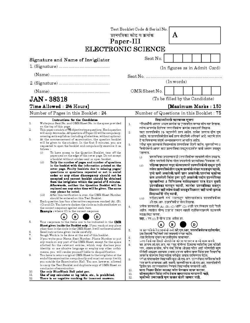
A
ELECTRONIC SCIENCE
Signature and Name of Invigilator Seat No.
1. (Signature) ......................................... (In figures as in Admit Card)
(Name) ................................................ Seat No. ..............................................................
2. (Signature) ......................................... (In words)
(Name) ................................................ OMR Sheet No.
JAN - 38318 (To be filled by the Candidate)
Time Allowed : 2½ Hours] [Maximum Marks : 150
Number of Pages in this Booklet : 24 Number of Questions in this Booklet : 75
Instructions for the Candidates
1. Write your Seat No. and OMR Sheet No. in the space provided 1.
on the top of this page.
2. This paper consists of 75 objective type questions. Each question
will carry two marks. All questions of Paper-III will be compulsory, 2.
covering entire syllabus (including all electives, without options).
3. At the commencement of examination, the question booklet
will be given to the student. In the first 5 minutes, you are
requested to open the booklet and compulsorily examine it as 3.
follows :
(i) To have access to the Question Booklet, tear off the
paper seal on the edge of this cover page. Do not accept
(i)
a booklet without sticker-seal or open booklet.
(ii) Tally the number of pages and number of questions
in the booklet with the information printed on the (ii)
cover page. Faulty booklets due to missing pages/
questions or questions repeated or not in serial
o rder or any other discre pancy should not be
accepted and correct booklet should be obtained
from the invigilator within the period of 5 minutes.
Afterwards, neither the Question Booklet will be
replaced nor any extra time will be given. The same
may please be noted.
(iii) After this verification is over, the OMR Sheet Number
should be entered on this Test Booklet. (iii)
4. Each question has four alternative responses marked (A), (B),
(C) and (D). You have to darken the circle as indicated below on
the correct response against each item. 4. (A), (B), (C) (D)
Example : where (C) is the correct response.
A B D
(C)
5. Your responses to the items are to be indicated in the OMR
Sheet given inside the Booklet only. If you mark at any place A B D
other than in the circle in the OMR Sheet, it will not be evaluated.
5.
6. Read instructions given inside carefully.
7. Rough Work is to be done at the end of this booklet.
8. If you write your Name, Seat Number, Phone Number or put 6.
any mark on any part of the OMR Sheet, except for the space 7.
allotted for the relevant entries, which may disclose your 8.
identity, or use abusive language or employ any other unfair
means, you will render yourself liable to disqualification.
9. You have to return original OMR Sheet to the invigilator at the
end of the examination compulsorily and must not carry it with 9.
you outside the Examination Hall. You are, however, allowed
to carry the Test Booklet and duplicate copy of OMR Sheet on
conclusion of examination.
10. Use only Blue/Black Ball point pen. 10.
11. Use of any calculator or log table, etc., is prohibited. 11.
12. There is no negative marking for incorrect answers. 12.
Page 2
Page 3
Paper III
Time Allowed : 2½ Hours] [Maximum Marks : 150
Note : This paper contains Seventy Five (75) multiple choice questions, each
question carrying Two (2) marks. Attempt All questions.
1. If the temperature of a semi- 3. If a full wave rectifier circuit is
conductor diode increases, then operating from 50 Hz mains, then
leakage current ......................... the fundamental frequency in the
(A) remains the same ripple will be :
(B) decreases (A) 25 Hz
(C) increases (B) 50 Hz
(D) becomes zero (C) 70.7 Hz
2. If the base current is 30 A and (D) 100 Hz
current gain is 50, then the collector 4. Thermal oxidation in IC fabrication
current will be : is a process carried out at :
(A) 15 mA (A) High temperature
(B) 1.5 mA (B) Low pressure
(C) 150 mA (C) Sub zero temperature
(D) 1.5 A (D) Room temperature
3 [P.T.O.
Page 4
the correct answer using codes given the correct answer using codes given
below : below.
List I List I
(a) BJT (a) Ion Implantor
(b) JFET (b) CVD Reactor
(c) ZENER diode (c) UV Exposure
(d) MOSFET (d) Pad to pin connection
List II List II
(i) High (i) Photolithography
(ii) Voltage regulator (ii) Conductor and directric film
(iii) Insulated gate voltage deposition
controlled current (iii) Bonding
(iv) Reverse biased gate (iv) Doping
Codes : Codes :
(a) (b) (c) (d) (a) (b) (c) (d)
(A) (iv) (ii) (iii) (i) (A) (i) (iii) (ii) (iv)
(B) (i) (iii) (ii) (iv) (B) (ii) (iv) (i) (iii)
(C) (ii) (iv) (iii) (i) (C) (iv) (ii) (i) (iii)
(D) (i) (iv) (ii) (iii) (D) (iii) (ii) (i) (iv)
4
Page 5
a network has the pole-zero locations
control system shows the gain to be
as shown in the following figure. If
Z(o) = 3, then Z(s) is : –20 dB at the phase cross over
frequency. What is the gain margin
expressed as a ratio ?
(A) 1
(B) 5
(A) 3 (s+3) | (s2+2s+3)
(B) 2 (s+3) | (s2+2s+2) (C) 10
(C) 3 (s–3) | (s2–2s–2) (D) 20
(D) 2 (s–3) | (s2–2s–3)
10. Laplace transform of (t–T) is :
8. Z-transform of x (–n) is :
(A) constant
(A) X (Z)
(B) 1|e–sT
(B) X (Z–2)
(C) e–sT
(C) X (n)
(D) X (Z–1) (D) s e–sT
5 [P.T.O.
Page 6
select the correct answer using the
select the correct answer using the
codes given below :
codes given below :
List I
(a) hfe List I
(b) hoe (a) Voltage gain = 10
(c) hie
(b) Power gain = 10
(d) hre
(c) Power gain = 1000
List II
(d) Voltage gain = 100
vbe
(i) vce I List II
B constant
vbe (i) 10 dB
(ii) ib V
ce constant
(ii) 40 dB
ic
(iii) 30 dB
(iii) vce I
b constant
(iv) 20 dB
ic
(iv) ib V Codes :
ce constant
Codes : (a) (b) (c) (d )
(a) (b) (c) ( d) (A) (iv) (i) (ii) (iii)
(A) (iv) (ii) (i) (iii) (B) (i) (iv) (iii) (ii)
(B) (iv) (i) (ii) (iii)
(C) (i) (iv) (ii) (iii)
(C) (ii) (iii) (iv) (i)
(D) (iv) (i) (iii) (ii)
(D) (iv) (iii) (ii) (i)
6
Page 7
configuration of : fixed voltage regulator can be
increased :
(A) Open loop op-amp (A) Adding external pass transistor
(B) Differential input op-amp (B) By increasing ground pin
voltage
(C) Positive feedback op-amp (C) Cascading with another 3-pin
voltage regulator
(D) Negative feedback op-amp
(D) Using voltage doubler at input
14. ID and VGS notations in a FET 17. Match the List-I with List II and
select the correct answer using the
denote the following parameters :
codes given below :
(A) Total instantaneous values List I (Configuration
Configuration)
Configuration :
(a) Common emitter
(B) Instantaneous ac values
(b) Common collector
(C) Phasor values (c) Common base
(d) Emitter follower
(D) DC values
List II (Characteristics
Characteristics)
Characteristics :
15. For fabrication of current mirror in (i) High input resistance
an integrated circuit the following (ii) Low output resistance
components are required : (iii) Moderate input resistance
(iv) Low input resistance
(A) Two transistors
Codes :
(B) One transistor and one (a) (b) (c) (d )
MOSFET (A) (i) (iii) (iv) (ii)
(B) (i) (ii) (iii) (iv)
(C) Two transistors in super mode (C) (iii) (ii) (iv) (i)
(D) One transistor and Al reflector (D) (iv) (ii) (i) (iii)
7 [P.T.O.
Page 8
select the correct answer using the offset voltage equal to 1/2 LSB is
added to the D/A converter's output.
codes given below :
This is done to :
List I (A) Improve the speed of operation
(a) Voltage gain (B) Reduce maximum quantization
error
(b) Current gain
(C) Increase the number of bits at
(c) Power gain the output
(d) Output resistance (D) Increase the range of input
voltage that can be converted
List II
20. The main difference between JK and
(i) Very high CE RS flip-flop is that :
(ii) Very low in CC (a) JK flip-flop requires clock input
(iii) High in CB (b) There is a feedback in JK flip-
flop
(iv) Low in CB
(c) JK flip-flop accepts both inputs
Codes : as high
(d) JK flip-flop is similar to D-flip
(a) (b) (c) ( d)
flop
(A) (iii) (iv) (i) (ii)
(A) a and b
(B) (ii) (iii) (iv) (i) (B) b only
(C) (ii) (iv) (iii) (i) (C) a and c
(D) (ii) (iv) (i) (iii) (D) b and d
8
Page 9
when : correct answer from the codes given
below :
(a) The output is low
(a) GAL
(b) The output is high (b) PAL
(c) CPLD
(c) Clock is enabled
(d) FPGA
(d) Both reset and set input
(e) EEPROM
disabled
(i) Complex programmable logic
(A) (c) device
(ii) Field programmable gate array
(B) (a) and (b)
logic
(C) (a) and (c) (iii) Programmable array logic
(iv) Gate array logic devices
(D) (c) and (d)
(generic)
22. How many entries will be there in (v) Electrical erasable program-
the truth table of a 3 input NAND mable read only memory.
gate ? Codes :
(a) (b) (c) (d ) (e)
(A) 3
(A) (ii) (i) (iv) (iii) (v)
(B) 6
(B) (i) (ii) (iii) (iv) (v)
(C) 9 (C) (i) (iv) (iii) (v) (ii)
(D) (iv) (iii) (i) (ii) (v)
(D) 8
(E) (iii) (iv) (ii) (i) (v)
9 [P.T.O.
Page 10
select the correct answer using the instruction perform the move
codes given below : accumulator to external RAM of
16-bit address ?
List I
(A) MOV @ D PTR, A
(a) Sequential logic circuits
(B) MOV X @ Ri, A
(b) Combination logic circuits
(C) MOV A, @ Ri
(c) Synchronous sequential logic
(D) MOV X @ DPTR, A
(d) Asynchronous logic circuits
26. In 8085 microprocessor, RST 6
List II
instruction transfers program
(i) Independent of clock signal
execution to the following
(ii) Depends on clock signal location :
(iii) Combinational circuit with (A) 0024 H
storage element as feedback
(B) 0030 H
path
(C) 0048 H
(iv) Decoder, multiplexers
(D) 0060 H
Codes :
27. SIM instruction in 8085 stands
(a) (b) (c) ( d)
for :
(A) (ii) (iii) (i) (iv)
(A) select interrupt mask
(B) (iii) (iv) (ii) (i)
(B) sort interrupt mask
(C) (i) (iv) (iii) (ii)
(C) set interrupt mask
(D) (ii) (i) (iv) (iii)
(D) subscribe interrupt module
10
Page 11
and 'transmit' buffer in serial the correct answer using codes given
communication in 8051 is :
below :
(A) SCON
List I
(B) PCON
(C) SBUF (a) Port 0 (SFR 80 H)
(D) Accumulator (b) Port 1 (SFR 90 H)
29. Match List I with List II and select
(c) Port 2 (SFR A0 H)
the correct answer using codes given
below the list : (d) Port 3 (SFR B0 H)
List I
List II
(a) S1 = 0, S0 = 0
(b) S1 = 0, S0 = 1 (i) Quasi Bi-directional general
(c) S1 = 1, S0 = 0 purpose
(d) S1 = 1, S0 = 1 (ii) Content of DPL
List II
(iii) Serial data communication/
(i) OPCODE FETCH
interrupts
(ii) READ
(iv) External memory HIGH byte
(iii) HALT
(iv) WRITE Codes :
Codes : (a) (b) (c) (d )
(a) (b) (c) ( d)
(A) (ii) (i) (iii) (iv)
(A) (i) (ii) (iii) (iv)
(B) (iii) (iv) (ii) (i) (B) (ii) (i) (iv) (iii)
(C) (ii) (i) (iv) (iii) (C) (i) (ii) (iii) (iv)
(D) (iv) (i) (ii) (iii)
(D) (ii) (iv) (iii) (i)
11 [P.T.O.
Page 12
Assertion-Reason type questions : Tunnel diode is used as a memory
element.
The following items consist of two
Reason (R) :
statements, one labelled as
It has negative resistance
'Assertion (A)', and the other labelled characteristics due to quantum
the 'Reason (R)'. You are to examine mechanical effect.
these two statements and decide if 32. Assertion (A) :
the Assertion (A) and the Reason (R) Superposition theorem is not
applicable for power calculations.
are individually true and if so,
Reason (R) :
whether the reason is a correct
Power is a non-linear quantity.
explanation of the Assertion.
33. Assertion (A) :
Select your answer to these items
Op-amp has high input impedance.
using the codes given below and
Reason (R) :
mark your answer sheet accordingly.
Op-amps have low input offset
Codes : current.
34. Assertion (A) :
(A) Both (A) and (R) are true and
In order to synchronise a Mealy type
(R) is the correct explanation of
circuits the inputs of the sequential
(A) circuit must be synchronized with
(B) Both (A) and (R) are true but the clock and the outputs must be
sampled only during the clock edge.
(R) is not the correct
Reason (R) :
explanation of (A)
In Mealy model the outputs may
(C) (A) is true but (R) is false change if input changes during the
clock period and output may have
(D) (A) is false and (R) is true
momentary false values.
12
Page 13
PWM signal can be easily generated Graded index optical fibers are used
by 8051. for reasonably high band width
Reason (R) : application.
It has built in timer/count. Reason (R) :
36. Assertion (A) : Graded index fibers are designed to
The result of a logical and operations have low time dispersion.
in C will be true only if both 40. Assertion (A) :
operands are true.
A hot wire ammeter has a cramped
Reason (R) : scale.
The result of a logical or operations Reason (R) :
will be true if either operand is true
The heat is proportional to square
or if both operands are true.
of current.
37. Assertion (A) :
Read the following paragraph and
A stub is shorted or open section of
answer the question Nos. 41 to 45 :
transmission line used inconjun-
ction with transmission line. An oscillator having initially been
set at a particular frequency will
Reason (R) :
generally drift and wander about in
A stub cancel out reflections and
frequency. The frequency stability of
provide impedance match.
an oscillator is a measure of its
38. Assertion (A) : ability to maintain as nearly a fixed
From SNR point of view, FM is frequency as possible over as long
superior to PM by a factor of 3. a time as possible. These deviations
Reason (R) : of frequency arise because the
values of critical features, on which
Narrowband FM offers no
the oscillator frequency depends, do
improvement in SNR over AM.
13 [P.T.O.
Page 14
critical features include circuit dependence on the far larger number
components, transistor parameters, of features is comparatively slight.
supply voltage, stray capacitances For example the frequency of phase
etc. Accordingly, an obvious but shift oscillator primarily depends on
clearly useless solution of the R and C and other parameters do
not affect it too much. In a parallel
problem of making a frequency
resonant circuit the impedance
stable oscillator is to keep all these
changes from an inductive to a
features constant. In the first place,
capacitive reactance as the
the number of circuit features is very
frequency is increased through
large and some of the features like
resonance point. If the Q is infinite
transistor parameters are inherently this change in phase is abrupt.
unstable and extremely difficult to Hence a tuned circuit oscillator will
keep constant. Moreover, it is hard have excellent frequency stability
to know where stray circuit elements independent of temperature, current
and couplings are located and how etc.
to estimate their magnitudes. Thus 41. The frequency of any oscillator is :
making it difficult to maintain them (A) Unstable
constant.
(B) Constant
However, it is recognized that in (C) Not dependent on component
every oscillator circuit there are selection
relatively few circuit features on
(D) Decided by semiconductor
which the frequency is sensitively device only
14
Page 15
false statement ? oscillator :
(A) An oscillator would not produce (A) depends heavily on parasitic
components
constant frequency
(B) is decided basically by amplifier
(B) The tuned circuit oscillator is
gain
highly unstable
(C) depends primarily on R and C
(C) Transistor parameters are only
inherently unstable (D) is independent of temperature,
current etc.
(D) Stray circuit elements and
45. The tuned oscillator has excellent
couplings affect stability of frequency stability because :
oscillator (A) the frequency is basically
43. An effective solution to maintain decided by R and C
oscillation frequency highly stable (B) the change in phase is abrupt
due to high Q
is :
(C) supply voltage is highly stable
(A) Switch off the circuit
(D) stray capacitances are of large
(B) To identify the stray compo- value
nents and bypass them 46. A stream of type .................... can be
connected to a file with a call to the
(C) Choose a circuit configuration
member function open.
which does not have large
(A) ifstream
number of critical features
(B) ofstream
(D) Make the circuit impedance (C) both (A) & (B)
high
(D) object
15 [P.T.O.
Page 16
loop body at least .................. select the correct answer using the
(A) twice codes given below :
(B) three times List I
'C' Function
(C) once
(a) a cos (d)
(D) four times
(b) abs (i)
48. All subtasks in a program can be
(c) fprint (f, ..........)
implemented as functions, either as
(d) time (p)
functions that return a value or
as ..................... List II
Include File
(A) Return-function
(i) time.h
(B) Void-functions
(ii) stdio.h
(C) Call functions
(iii) math.h
(D) All of the above
(iv) stdlib.h
49. A ......................... is a program that Codes :
does nothing but test a function.
(a) (b) (c) (d )
(A) Hello program (A) (i) (ii) (iii) (iv)
(B) Print program (B) (iii) (iv) (ii) (i)
(C) Interrupt program (C) (iv) (iii) (ii) (i)
(D) Driver program (D) (ii) (iii) (iv) (i)
16
Page 17
select the correct answer using the 30 s wide and having an inter-
codes given below : pulse separation of 20 s is
List I propagating through a transmission
line. How long should the
Expression in 'C'
transmission line be in meters so
(a) dx + x that exactly three pulses are on the
(b) ((int) dx) + ix line at a time ? Assume propagation
(c) i + c speed to be 3 × 10⁸ m/s.
(d) x + c (A) 2.5 km
List II (B) 3.9 km
Data type (C) 25 km
(i) long integer (D) 39 km
(ii) double - precision 54. The Maxwell's equation
(iii) float or double float
(iv) integer D
H J cond for
t
Codes :
(a) (b) (c) ( d) free space becomes :
(A) (iv) (iii) (ii) (i) (A) H 0
(B) (i) (ii) (iv) (iii)
(B) H J cond
(C) (ii) (i) (iv) (iii)
(D) (iii) (iv) (ii) (i) D
(C) H
52. For a given rectangular wave guide, t
the cut-off frequency for TE10 mode (D) H infinite
is always :
55. Back bombardment of the cathode
(A) Lower than that for the TE11 occurs in ...................
mode
(A) Klystron
(B) Higher than that for the TE11
(B) Magnetron
mode
(C) Equal to that for the TE11 mode (C) Vacuum tubes
(D) Zero (D) GaAs FET
17 [P.T.O.
Page 18
the correct answer using codes given
the correct answer using codes given
below :
below :
List I
List I
(a) Maxwell's equation based on
Ampere's law (a) Gunn diode
(b) Maxwell's second equation
(b) GaAs FET
based on Faraday's law
(c) Maxwell's third equation based (c) Conventional transistor
on Gauss' law (d) Pin diode
(d) Maxwell's fourth equation
List II
based on non-existence of
magnetic monopole (i) exhibit stray capacitances and
List II inductances at higher
frequencies
(i) ·B 0
(ii) has small capacitance when
D
(ii) H J reverse biased
t
(iii) transferred electron device
(iii) ·D
(iv) used in low noise amplifier
B
(iv) E
t Codes :
Codes :
(a) (b) (c) (d )
(a) (b) (c) ( d)
(A) (iii) (iv) (i) (ii)
(A) (ii) (iv) (i) (iii)
(B) (iii) (iv) (ii) (i)
(B) (iv) (ii) (i) (iii)
(C) (iv) (iii) (ii) (i)
(C) (ii) (iv) (iii) (i)
(D) (i) (iii) (iv) (ii)
(D) (ii) (i) (iii) (iv)
18
Page 19
58. In FM superheterodyne receiver, the II and select the correct answer
beat frequency is : using the codes given below :
Column I
(A) 910 kHz (P) Low Pass Filter
(Q) High Pass Filter
(B) 455 kHz
(R) Band Pass Filter
(C) 21.14 MHz (S) FIR Filter
Column II
(D) 10.7 MHz
59. Superheterodyne AM receiver has :
(A) Delayed AGC
(B) AGC (1)
(C) No AGC
(D) Ideal AGC
60. A Hilbert transformer is a :
(A) Non-linear System
(B) Non-causal System (2)
(C) Time-varying System
(D) Low Pass System
61. Consider the following system :
(3)
Impulse response h(t ) is a filter
matched to x ( t ). The Fourier
transform of the output y(t) shall
be : (4)
(A) e f2
(B) e 2 f 2 Codes :
(A) P–3, Q–1, R–2, S–4
(C) e f 22 (B) P–1, Q–3, R–2, S–4
(C) P–1, Q–3, R–4, S–2
(D) e |f | (D) P–3, Q–1, R–4, S–2
19 [P.T.O.
Page 20
with RL circuit can be reduced
II and select the correct answer
by :
using the codes given below :
(a) increasing circuit resistance R
Column I (b) decreasing circuit resistance R
(c) increasing circuit inductance L
(P) Km (t) A sin ( ct)
(d) decreasing circuit inductance L
(Q) A sin [ ct + Km(t)]
Options :
(R) [1 + Km (t)] A sin ( ct) (A) b and d
(B) a and d
t
(S) A sin ct K m(t)d (C) b and c
–
(D) d only
Column II
65. For an SCR with turn-on time of 5 s,
(W) PM an ideal trigger pulse should
have :
(X) FM
(A) Short rise time with pulse width
(Y) AM
= 3 s
(Z) DSBSC (B) Long rise time with pulse width
= 6 s
(A) P–Z, Q–W, R–Y, S–X
(C) Short rise time with pulse width
(B) P–W, Q–Z, R–Y, S–X
= 6 s
(C) P–X, Q–W, R–Z, S–Y (D) Long rise time with pulse width
(D) P–Y, Q–Z, R–W, S–X = 3 s
20
Page 21
the correct answer using codes given optical communication :
below :
(i) Modulator
List I
(a) Single phase full bridge (ii) Wavelength Division Multiplexer
inverter
(iii) Repeaters
(b) Power device combining BJT
and MOSFET (iv) Time Division Multiplexer
(c) Device conducting during OFF The correct sequence of their
period of SCR
placement from transmission side
(d) Circuit used for converting low
is :
voltage dc to high voltage dc
List II (A) (i) (iii) (ii) (iv)
(i) step up chopper (B) (ii) (iii) (iv) (i)
(ii) free wheeling diode
(C) (iv) (ii) (i) (iii)
(iii) IGBT
(D) (i) (iv) (ii) (iii)
(iv) can be operated in Load
commutation mode 68. The following is the most important
Codes : requirement for laser :
(a) (b) (c) ( d)
(A) Optical pumping
(A) (i) (ii) (iii) (iv)
(B) (ii) (iii) (iv) (i) (B) Stimulated emission
(C) (iii) (ii) (i) (iv) (C) Positive feedback
(D) (iv) (iii) (ii) (i) (D) Current modulation
21 [P.T.O.
Page 22
the correct answer using codes given piezoelectric substances ?
below : (1) Barium titanate
List I (2) Lead titanate
(Optical Wavelength) (3) Lead zirconate
(a) 1440 nm (4) Cadmium and sulphate
(b) 850 nm (A) 1, 2 and 4
(c) 1300 nm
(B) 1, 3 and 4
(d) 1550 nm
(C) 1, 2 and 3
List II
(D) 2, 3 and 4
(i) Low loss
72. Match List I with List II and select
(ii) High speed
the correct answer using codes given
(iii) High loss
below :
(iv) Low cost
List I
Codes :
(a) Electron microscope
(a) (b) (c) ( d)
(b) Oscilloscope
(A) (i) (ii) (iv) (iii)
(c) Galvanometric recorder
(B) (iv) (i) (ii) (iii)
(d) Magnetic recorder
(C) (iii) (iv) (ii) (i)
(D) (i) (ii) (iv) (iii) List II
70. The drawbacks of strain gauges (i) Electron gun
are : (ii) Condensing magnetic lens
S1 : Low fatigue life (iii) Recording head
S2 : They are expensive, brittle (iv) Drive motor
and sensitive to temperature Codes :
S3 : Poor linearity (a) (b) (c) (d )
(A) S1 and S2 (A) (ii) (iv) (i) (iii)
(B) S2 and S3 (B) (ii) (iii) (i) (iv)
(C) S1 and S3 (C) (iii) (ii) (iv) (i)
(D) S1 only (D) (ii) (i) (iv) (iii)
22
Page 23
the correct answer using codes given
shown in the following figure is :
below :
List I
(Characteristic Equation of
the System)
(a) s5 + s4 + 2s3 + 2s2 + 3s + 15 = 0
(A) Type : 1, Order : 3
(b) s6 + 2s5 + 8s4 + 12s3 + 20s2 +16s
(B) Type : 3, Order : 1 + 16 = 0
(C) Type : 2, Order : 2 (c) G(s) H(s) = 10/s (s + 2) (s + 5)
(D) Type : 1, Order : 1 s+5
(d) G(s) = s2 + 4s + 9
74. Consider the following statements
regarding root loci.
List II
(1) All root loci start from the
(Stability of the System)
respective poles of G (s) H (s)
(i) marginally stable
(2) All root loci end at the respective
(ii) unstable
zeros of G(s) H(s) or go to
(iii) stable
infinity.
(iv) phase angle of the system varies
(3) The root loci are symmetrical
between 0° and –90°.
about the imaginary axis of the
S-plane. Codes :
(a) (b) (c) (d )
Of these statements :
(A) (ii) (i) (iii) (iv)
(A) 1, 2 and 3 are correct
(B) (i) (ii) (iii) (iv)
(B) 1 and 2 are correct
(C) (iii) (iv) (i) (ii)
(C) 2 and B are correct
(D) (iv) (iii) (ii) (i)
(D) 1 and 3 are correct
23 [P.T.O.
Page 24
24
Document Details
| Board / Org | Maharashtra Exams |
| Exam | MAHA SET |
| Type | Question Paper |
| Pages | 24 |
| Updated | 30 Apr 2026 |