PU CET PG 2017 Question Paper M.E._Electronics_ Communication Engg._
Finished viewing? Save it for later —
Download PU CET PG 2017 Question Paper M.E._Electronics_ Communication Engg._ (PDF · 10 pages)About PU CET PG 2017 Question Paper M.E._Electronics_ Communication Engg._
PU CET PG 2017 Question Paper M.E._Electronics_ Communication Engg._ is available here for free download. Published by Punjab University for PU CET PG, this question paper can be viewed online or downloaded as a PDF (10 pages). Candidates preparing for PU CET PG can use PU CET PG 2017 Question Paper M.E._Electronics_ Communication Engg._ to understand the exam pattern, the type of questions asked, and the overall difficulty level.
Frequently Asked Questions
How can I download PU CET PG 2017 Question Paper M.E._Electronics_ Communication Engg._?
Open this page and click the Download button to save PU CET PG 2017 Question Paper M.E._Electronics_ Communication Engg._ as a PDF. It is completely free on AglaSem Docs.
Is PU CET PG 2017 Question Paper M.E._Electronics_ Communication Engg._ free to download?
Yes. PU CET PG 2017 Question Paper M.E._Electronics_ Communication Engg._ can be viewed online and downloaded as a PDF free of cost on AglaSem Docs.
How many pages does PU CET PG 2017 Question Paper M.E._Electronics_ Communication Engg._ have?
PU CET PG 2017 Question Paper M.E._Electronics_ Communication Engg._ contains 10 pages, which you can read online or download together as a single PDF.
Where can I find more PU CET PG study material?
You can find more PU CET PG question papers, sample papers, syllabus, and answer keys on AglaSem Docs.
PU CET PG 2017 Question Paper M.E._Electronics_ Communication Engg._ – Text
Read the full text of this question paper below — useful to quickly search, copy and reference the content online without downloading the PDF.
📄 View text version (10 pages)
Page 1
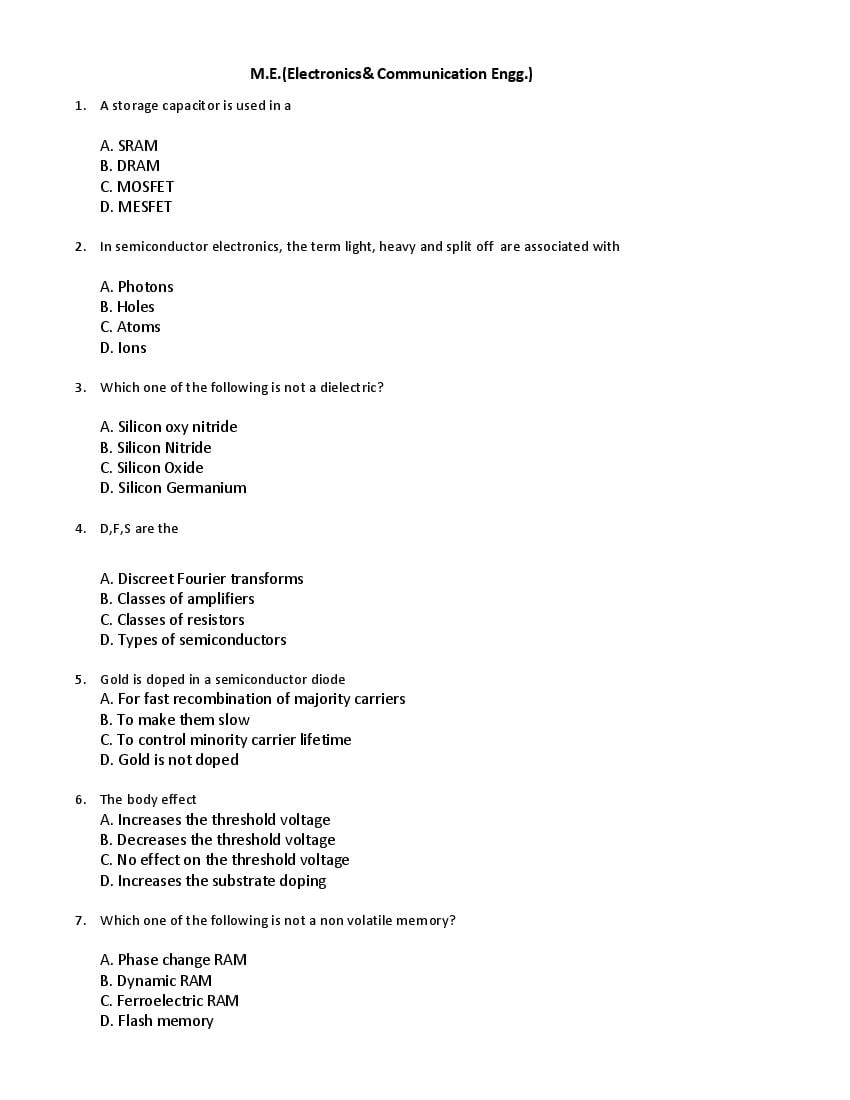
1. A storage capacitor is used in a
A. SRAM
B. DRAM
C. MOSFET
D. MESFET
2. In semiconductor electronics, the term light, heavy and split off are associated with
A. Photons
B. Holes
C. Atoms
D. Ions
3. Which one of the following is not a dielectric?
A. Silicon oxy nitride
B. Silicon Nitride
C. Silicon Oxide
D. Silicon Germanium
4. D,F,S are the
A. Discreet Fourier transforms
B. Classes of amplifiers
C. Classes of resistors
D. Types of semiconductors
5. Gold is doped in a semiconductor diode
A. For fast recombination of majority carriers
B. To make them slow
C. To control minority carrier lifetime
D. Gold is not doped
6. The body effect
A. Increases the threshold voltage
B. Decreases the threshold voltage
C. No effect on the threshold voltage
D. Increases the substrate doping
7. Which one of the following is not a non volatile memory?
A. Phase change RAM
B. Dynamic RAM
C. Ferroelectric RAM
D. Flash memory
Page 2
A. Semiconductor
B. Metal
C. Insulator
D. Gas
9. GST is a
A. Material for memories
B. A standard for packaging
C. Communication protocol
D. Type of transistor
10. Which one of the following is true for an HBT?
A. It is a class of field effect transistors
B. Used at low frequencies
C. Uses germanium in the base
D. It is a class of resistors
11. A program counter in 8085 microprocessor is a
A. 16 bit register
B. 8 bit register
C. 32 bit register
D. 64 bit register
12. The difference of the contact potential in a silicon diode and a germanium diode is
approximately (mV)
A) 700
B) 400
C) 100
D) 1000
13. In a MOSFET, moderate and weak are types of
A. Amplifiers
B. Inversion mode
C. Depletion mode
D. Accumulation mode
14. Low k dielectrics are used in
A. Interconnect technology
B. Gate oxide
C. Field oxide
D. Substrate
15. MNOS and NMOS are
A. Class of dielectrics
Page 3
C. Same
D. Memory and a transistor
16. Which of the following are the advantages of a closed loop control system?
A. Reduces the overall gain
B. Complex and costly
C.Oscillatory response
D. Less affected with noise
17. Which of these logic gates act as universal gates?
A. NOR, XNOR
B. OR, NOT
C. NOR, NAND
D. XOR, NOR
18. Which logic family consumes least power?
A. TTL
B. CMOS
C.RTL
D.DTL
19. A digital circuit that can store a bit is a
A. NOR gate
B. Flip-flop
C. NAND gate
D. XOR gate
20. Crystal oscillator
A. Uses piezoelectric effect
B. Used in AM transmitters
C. Produces stable frequency
D. All of the above
21. The oscillator used for LF applications
A. LC
B. RLC
C. RC
D. MFC
22. Transit time effect is present in
A. Gunn diode
B. Tunnel diode
C. Junction diode
D. MOSFET
23. A single PMOS can be used as
A. CMOS inverter
B. NAND gate
C. Transmission gate
D. Pass transistor
Page 4
A. Eber Moll
B. Gummel poon
C. BSIM
D. MIS
25. Schottky diodes have
A. Planar technology
B. Au-Si contact
C. 0.3V as contact potential
D. All of the above
26. An Op-Amp comparator uses
A. Positive feedback.
B. Negative feedback
C. Both negative and positive feedback
D. No need of feedback
27. DCTL stands for
A. Direct coupled transistor logic
B. Diode coupled transistor logic
C. Diode circuit type logic
D. Direct coiled transistor logic
28. GaAs is generally used in
A. MESFET
B. Gunn diode
C. LED
D. All
29. Electric field inside a hollow conducting sphere is
A. Zero
B. Non zero but constant
C. Vary with the radius of sphere
30. IGBT and GTO are
A. Communication protocols
B. Power devices
C. MOSFETs
D. CMOS inverter types
31 The amount of time between the creation and disappearance of a free electrons is called
A. Lifetime
B. Recombination
C. Generation
D. Transit time
Page 5
A. Parallel combination of MOS transistors
B. Serial combination of MOS transistors
C. Crisscross combination of MOS transistors
D. Parallel and serial combination of MOS transistors
33. SiC is used for
A. High temperature applications
B. Low temperature applications
C. As a dielectric
34. Class C amplifier
A. Produces distortion
B. Conducts for less than half the cycle
C. Highly efficient
D. All
35. If holding current of a thyristor is 1mA then latching current is of the order of
A. 1m A
B. 2mA
C. 0.5mA
D. 0.1mA
36. Quantization error occurs in
A. AM signals
B. Noise signals
C. PCM signals
D. FM signals
37. Reflex Klystron is a
A. Tubular device
B. Low power microwave generator
C. Two cavity device
D.All
38. A BJT works because
A. Base is kept thin
B. Base is kept thick
C. Base is highly doped
39. No of comparators present in an 8 bit flash
type ADC?
A. 256
B. 128
C. 255
D. 127
Page 6
A. MOSFET and a Junction diode
B. LED and a photodiode
C. BJT and a MOSFET
D. GTO and MOSFET
41. Language used for programming an FPGA
A. HDVL
B. Verilog
C. LHVD
D. Antilog
42. DIBL occurs in
A. Long channel MOSFET
B. Short channel MOSFET
C. BJT
43. GAA is a type of
A. Diode
B. MOSFET
C. BJT
D. Capacitor
44. Kirk effect occurs in
A. Diode
B. MOSFET
C. BJT
D. Capacitor
45. Gain-bandwidth product in a closed loop feedback system is
A. Constant
B. Variable with gain
C. Variable with bandwidth
46. Schering bridge and Hay’s bridge are used to measure
A. Frequency and inductance
B. Capacitance and inductance
C. Capacitance and resistance
D. Resistance and mutual inductance
47. The number of software interrupts in a 8085 microprocessor is
A. Five
Page 7
C. Seven
D. Six
48. Immediate and Direct are the
A. Addressing modes
B. Registers
C. Memory storage types
D. Interrupts
49. The difference in the number of pins (for interrupt) on a 8085 chip and the number of interrupts is
A. Zero
B. One
C. Two
D. Three
50. No. of pins in 8085 microprocessor is
A. 38
B. 40
C. 42
D. 36
51. In 8085, 16 bit register is
A. Instruction register
B. Stack pointer
C. Accumulator
52. Flags in a 8085 microprocessor are
A. 4
B. 5
C. 3
D. 6
53. In 8085, the ALE is a
A. Control signal
B. Data signal
C. Address signal
54. The DMA controller chip number is
A. 8237
B. 8085
C. 8225
D. 8155
55. The intrinsic impedance of free space is
approximately
Page 8
B. 277 0hms
C. 377 ohms
D. 477 ohm
56. Intrinsic region in a PIN diode makes it suitable for
A. Photo detecting applications
B. Rectifying applications
C. Maximum absorption of Electrons
D. Minimum absorption of Electrons
57. Super position theorem is not used to calculate
A. Power
B. Voltage
C. Current
D. Resistance
58. KCL works on the principle of conservation of
A. Charge
B. Power
C. Energy
D. Voltage
59. Total internal reflection occurs
A. On a glass surface
B. In a optical fiber cable
C. In a Cu cable
D. In an Al cable
60. Dynamic impedance of an ideal tank circuit is
A. Zero
B. Infinite
C. Depends on L
D. Depends on C
61. A resistor stores energy in the form of
A. Electric field
B. Magnetic field
C. Electromagnetic fields
62. Automatic control system is also called as
Page 9
B. Open loop control system
C. Both A and B
63. Power density in an antenna is
A. Reflected power per unit area
B. Refracted power per unit area
C. Radiated power per unit area
64. MASER is used in
A. Atomic clocks
B. Radio telescopes
C. Space applications
D. All
65. Light emitting diode can be fabricated using
A.III-V compounds
B. Organic polymers
C. Nanocrystals
D. All of the above
66. Sterdian is a measurement unit of
A. Solid angle
B. Planar angle
C. Square angle
D. Tri-angle
67. A capacitor in a steady state acts as
A. Open circuit
B. Short circuit
C. Resistor
D. Current source
68. --------------- is greater than critical frequency by a factor of secθ.
A. LUF
B. HUF
C. MUF
D. UHF
69. Antenna power gain is
A. Less than directivity
B. More than directivity
C. Can be both A and B
D. Neither A nor B
Page 10
A. Carrier mobility
B. Carrier charge
C. Mass
71. Elliptical, Chebyshev, Bessel, Cauer represent
A. AM transmitters
B. Analog filters
C. Rectifiers
D. Transistors
72. An RC coupled amplifier has an open loop gain of 100 and a lower cutoff frequency of 60 Hz. If
negative feedback with (β=0.2) is used, the lower cut off frequency (Hz) will be about
A. 60
B. 50
C. 2.8
D. 1.8
73. If a PMOS transistor replaces NMOS transistor in a circuit under same conditions,
A. ON current will increase
B. ON current will decrease
C. No change in analysis
D. Just sign of the calculated values will change
74. 2 input CMOS AND gate requires
A. 2 NMOS and 1 PMOS
B. 3 NMOS and 3 PMOS
C. 1 NMOS and 2 PMOS
D. 1 NMOS and 1 PMOS
75. 2 input CMOS OR gate requires
A. 2 NMOS and 1 PMOS
B. 3 NMOS and 3 PMOS
C. 1 NMOS and 2 PMOS
D. 1 NMOS and 1 PMOS
Document Details
| Board / Org | Panjab University |
| Exam | PU CET PG |
| Type | Question Paper |
| Pages | 10 |
| Updated | 22 Jul 2026 |