Karnataka SSLC Answer Key April 2019 Elements of Electronics Engineering
Finished viewing? Save it for later —
Download Karnataka SSLC Answer Key April 2019 Elements of Electronics Engineering (PDF · 8 pages)About Karnataka SSLC Answer Key April 2019 Elements of Electronics Engineering
Karnataka SSLC Answer Key April 2019 Elements of Electronics Engineering is available here for free download. Published by Karnataka Board for Class 10, this answer key can be viewed online or downloaded as a PDF (8 pages). Candidates preparing for Class 10 can use Karnataka SSLC Answer Key April 2019 Elements of Electronics Engineering to understand the exam pattern, the type of questions asked, and the overall difficulty level.
Frequently Asked Questions
How can I download Karnataka SSLC Answer Key April 2019 Elements of Electronics Engineering?
Open this page and click the Download button to save Karnataka SSLC Answer Key April 2019 Elements of Electronics Engineering as a PDF. It is completely free on AglaSem Docs.
Is Karnataka SSLC Answer Key April 2019 Elements of Electronics Engineering free to download?
Yes. Karnataka SSLC Answer Key April 2019 Elements of Electronics Engineering can be viewed online and downloaded as a PDF free of cost on AglaSem Docs.
How many pages does Karnataka SSLC Answer Key April 2019 Elements of Electronics Engineering have?
Karnataka SSLC Answer Key April 2019 Elements of Electronics Engineering contains 8 pages, which you can read online or download together as a single PDF.
Where can I find more Class 10 study material?
You can find more Class 10 question papers, sample papers, syllabus, and answer keys on AglaSem Docs.
Karnataka SSLC Answer Key April 2019 Elements of Electronics Engineering – Text
Read the full text of this answer key below — useful to quickly search, copy and reference the content online without downloading the PDF.
📄 View text version (8 pages)
Page 1
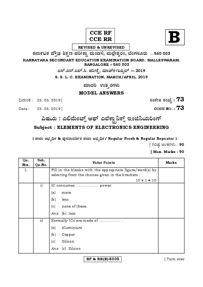
CCE RR
REVISED & UNREVISED
B
O⁄´¤%lO⁄ ÆË√v⁄ ÃO⁄–y Æ⁄¬fiO¤– »⁄flMs⁄ÿ, »⁄fl≈Ê«fiÀ⁄ ¡⁄M, ∑ÊMV⁄◊⁄‡¡⁄fl — 560 003
KARNATAKA SECONDARY EDUCATION EXAMINATION BOARD, MALLESWARAM,
BANGALORE – 560 003
G—È.G—È.G≈È.“. Æ⁄¬fiOÊ⁄–, »⁄·¤^È%/HØ√≈È — 2019
S. S. L. C. EXAMINATION, MARCH/APRIL, 2019
»⁄·¤•⁄¬ D}⁄ °¡⁄V⁄◊⁄fl
MODEL ANSWERS
¶´¤MO⁄ : 23. 03. 2019 ] —⁄MOÊfi}⁄ —⁄MSÊ¿ : 73
Date : 23. 03. 2019 ] CODE NO. : 73
…Œ⁄æ⁄fl : GΔ»ÊflMmÈ” A±È G≈ÊO¤oÒ¨OÈ” BMf¨æ⁄fl¬MVÈ
Subject : ELEMENTS OF ELECTRONICS ENGINEERING
( À¤≈¤ @∫⁄¥¿£% & Æ⁄‚¥´⁄¡¤»⁄~%}⁄ À¤≈¤ @∫⁄¥¿£%/ Regular Fresh & Regular Repeater )
[ V⁄¬Œ⁄r @MO⁄V⁄◊⁄fl : 90
[ Max. Marks : 90
Qn. Sub.
Value Points Marks
Nos. Qn.No.
1. Fill in the blanks with the appropriate figure/word(s) by
selecting from the choices given in the brackets :
10 × 1 = 10
i) IC consumes ................... power.
(a) more
(b) less
(c) none of these.
Ans. (b) less
ii) Normally ICs are made of .................. .
(a) Aluminium
(b) Copper
(c) Silicon.
Ans. (c) Silicon
RF & RR(B)-8005 [ Turn over
Page 2
Value Points Marks
iii) ICs are generally in the form of ................... .
(a) Flat pack
(b) Triangle
(c) Sphere.
Ans. (a) Flat pack
iv) IC 741 is an example of .................... .
(a) MOSFET
(b) Op-Amp
(c) FET.
Ans. (b) Op-Amp
v) Op-Amp has ................ impedance.
(a) low
(b) medium
(c) high.
Ans. (c) high
vi) Octal number system has ................... logic symbols.
(a) 8
(b) 4
(c) 6.
Ans. (a) 8
vii) If the inputs of NAND gate IC are 1 & 1 then its output
is ............... .
(a) 1
(b) 0
(c) 2.
Ans. (b) 0
viii) Binary number 0111 represents .................. .
(a) 9
(b) 8
(c) 7.
Ans. (c) 7
ix) .................. is used to store binary word temporary.
(a) Buffer register
(b) SISO register
(c) SIPO register.
Ans. (a) Buffer register
x) .................. is used to count number of clock pulses
arrived at its input.
(a) Inverter
(b) Counter
(c) Converter.
Ans. (b) Counter
Page 3
Value Points Marks
2. a) List any two active components. 2
i) Triode 2×1=2
ii) SCR (each 1)
b) Explain monolithic IC. 3
The most popular type of IC is monolithic IC. It consists
of capacitor, resistor, diode and transistor. All these
components are made on a fine wafer which is called
wafer. This type of IC are used widely.
3
c) Draw a neat sketch to show the construction of
monolithic IC. 5
Sketch - 4
Parts - 1 5
3. a) Define the term SSI. 2
SSI — Small Scale Integration, it contains up to
12 gates / unit
2
b) Describe how registors are fabricated in IC. 3
For making resistor, nichrome or eureka is diffused in
the wafer to form P2 region. This P2 region is made inside
an already made N2 region. Second terminal of the
resistor is connected to another element. 3
RF & RR(B)-8005 [ Turn over
Page 4
Qn. Sub.
Value Points Marks
Nos. Qn.No.
c) Draw a neat sketch of CRT. 5
Sketch - 4
Parts - 1 5
4. a) List types of ICs based on manufacturing process. 2
i) Monolithic
ii) Thin film
iii) Thick film
iv) Hybrid
2×1=2
b) Describe how hybrid ICs are differ from monolithic IC. 3
Hybrid IC is the combination of thick and thin film IC, it
differs from monolithic IC because of size, i.e. hybrid ICs
are of more weight also occupies more space. 3
c) Why ICs need less power to operate and more reliable
than discrete components ? 5
IC works on less power because, thousands of
components Ex : resistor, capacitor, diode etc. are
fabricated in small area even single square inch of chip
and using IC wiring becomes simple and solderless
circuit, hence all these reasons IC works on less power.
5
5. a) What is meant by an Op-Amp ? 2
Op-Amp generally written as operational amplifier, it is a
direct coupled high gain amplifier. 2
Page 5
Value Points Marks
b) Explain Inventing amplifier. 3
Inverting amplifier inverts the phase of the applied
signal, in which input Vin is applied to the inverting
terminal and non-inverting terminal is grounded, so it is
called inverting amplifier
i.e. V 0 = − A Vin 3
c) Draw the block diagram of an Op-Amp and explain input
stage. 5
Block diagram of an Op-Amp :
Input stage is having dual inputs, but balanced output
differential amplifier, it provides voltage gain of the
amplifier.
Diagram - 2
Notes - 3 5
6. a) Name the IC which inverts input data. 2
'NOT' gate IC always inverts input signal i.e. if the input
is '1' then its output is '0'. 2
b) Describe about universal logic gates. 3
'NAND' gate & 'NOR' gate are known as universal
building blocks or universal gates. This is because using
only 'NAND' gates or 'NOR' gates, we can produce many
logic functions. 3
RF & RR(B)-8005 [ Turn over
Page 6
Qn. Sub.
Value Points Marks
Nos. Qn.No.
c) Determine the values of
i) 6 – 4 by using binary subtraction method
ii) 24 + 8 by using binary addition method. 5
i) Determination of 6 – 4
Decimal subtraction Binary subtraction
6 0110
–4 – 0100
=2 = 0010
ii) Determination of 24 + 8
Decimal addition Binary addition
24 1 ← carry
+ 8 11000
= 32 1000
100000 2 + 2 = 5
7. a) How many digits are used in octal number system ? 2
The octal number system has a base of 8 i.e. it uses
8 digits, normally these are 0, 1, 2, 3, 4, 5, 6 and 7. 2
b) Why binary number system is most popular ? 3
The early computers employed decimal system but now-
a-days new system called binary system. The main
reason of utility is based on the fact that an electrical
circuit has only two states off & on or 0 & 1. In this way
this system is more popular. 3
c) Convert octal numbers (512)8 and (1035)8 into decimal
numbers. 5
i) (1035 )8 to decimal number
(1035 )8 = 5 × 8 0 + 3 × 81 + 0 × 8 2 + 1 × 8 3
= 5 + 24 + 0 + 512
= (541)10
ii) (512)8 into decimal number
(512)8 = (2 × 8 0 ) + (1 × 81 ) + (1 × 8 2 )
= 2 + 8 + 320
= (330)10 2 + 2 = 5
Page 7
Value Points Marks
8. a) Define the term flip-flop. 2
Flip-flop is a basic memory element. It has two stable
states i.e. its output is either 0 or 1. 2
b) Explain JK flip-flop. 3
JK flip-flop is a modified form of RS flip-flop, it removes
the forbidden condition (R = 1 & S = 1) of RS flip-flop. In
a RS flip-flop, the state with R = 1 & S = 1 is invalid,
whereas in JK flip-flop the O/P Q and Q is available.
These are used in counter. 3
c) Draw a neat diagram of RS flip-flop using NAND gates
and explain. 5
RS flip-flop
RS flip-flop is a Set-Reset flip-flop with which we can
store a desired specific state. It has two inputs R & S and
two outputs Q & Q , the input S is called sit and R is
referred as reset or clear input.
Diagram - 3
5
Explain - 2
9. a) What do you mean by microprocessor ? 2
A microprocessor is an IC chip which can act as
central processing unit of a digital computer, it contains
40 pins. 2
b) Explain 8085 microprocessor. 3
Intel 8085 microprocessor is a semiconductor device
consisting of electronic logic circuits manufactured by
using either a LSI or VLSI technique. It has various
sections such as, Interrupt control, Serial I/O control
etc. These are used in computers, instrumentation field
etc. 3
RF & RR(B)-8005 [ Turn over
Page 8
Value Points Marks
c) Explain Up and Down counter. 5
Counter is a special type of register, designed to count
the number of clock pulses arriving at its input.
Up counter counts upwards i.e. from 0000 to 1111 is
called an up counter such as a ripple counter.
Down counter counts downwards i.e. from 1111 to 0000
is called down counter. In this counter a preset signal is
amplified to all the flip-flops for setting them at 1111. 5
Document Details
| Board / Org | Karnataka Board |
| Exam | Class 10 |
| Type | Answer Key |
| Pages | 8 |
| Updated | 30 Apr 2026 |