MAHA SET 2015 Question Paper 3 Electronic Science
Finished viewing? Save it for later —
Download MAHA SET 2015 Question Paper 3 Electronic Science (PDF · 24 pages)About MAHA SET 2015 Question Paper 3 Electronic Science
MAHA SET 2015 Question Paper 3 Electronic Science is available here for free download. Published by Maharashtra Exams for MAHA SET, this question paper can be viewed online or downloaded as a PDF (24 pages). Candidates preparing for MAHA SET can use MAHA SET 2015 Question Paper 3 Electronic Science to understand the exam pattern, the type of questions asked, and the overall difficulty level.
Frequently Asked Questions
How can I download MAHA SET 2015 Question Paper 3 Electronic Science?
Open this page and click the Download button to save MAHA SET 2015 Question Paper 3 Electronic Science as a PDF. It is completely free on AglaSem Docs.
Is MAHA SET 2015 Question Paper 3 Electronic Science free to download?
Yes. MAHA SET 2015 Question Paper 3 Electronic Science can be viewed online and downloaded as a PDF free of cost on AglaSem Docs.
How many pages does MAHA SET 2015 Question Paper 3 Electronic Science have?
MAHA SET 2015 Question Paper 3 Electronic Science contains 24 pages, which you can read online or download together as a single PDF.
Where can I find more MAHA SET study material?
You can find more MAHA SET question papers, sample papers, syllabus, and answer keys on AglaSem Docs.
MAHA SET 2015 Question Paper 3 Electronic Science – Text
Read the full text of this question paper below — useful to quickly search, copy and reference the content online without downloading the PDF.
📄 View text version (24 pages)
Page 1
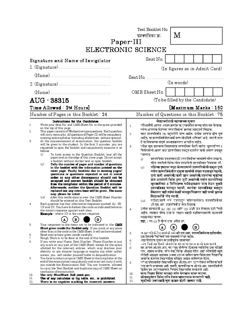
M
ELECTRONIC SCIENCE
Signature and Name of Invigilator Seat No.
1. (Signature) ......................................... (In figures as in Admit Card)
(Name) ................................................ Seat No. ..............................................................
2. (Signature) ......................................... (In words)
(Name) ................................................ OMR Sheet No.
AUG - 38315 (To be filled by the Candidate)
Time Allowed : 2½ Hours] [Maximum Marks : 150
Number of Pages in this Booklet : 24 Number of Questions in this Booklet : 75
Instructions for the Candidates
1. Write your Seat No. and OMR Sheet No. in the space provided 1.
on the top of this page.
2. This paper consists of 75 objective type questions. Each question
will carry two marks. All questions of Paper-III will be compulsory, 2.
covering entire syllabus (including all electives, without options).
3. At the commencement of examination, the question booklet
will be given to the student. In the first 5 minutes, you are
requested to open the booklet and compulsorily examine it as 3.
follows :
(i) To have access to the Question Booklet, tear off the
paper seal on the edge of this cover page. Do not accept
(i)
a booklet without sticker-seal or open booklet.
(ii) Tally the number of pages and number of questions
in the booklet with the information printed on the (ii)
cover page. Faulty booklets due to missing pages/
questions or questions repeated or not in serial
o rder or any other discre pancy should not be
accepted and correct booklet should be obtained
from the invigilator within the period of 5 minutes.
Afterwards, neither the Question Booklet will be
replaced nor any extra time will be given. The same
may please be noted.
(iii) After this verification is over, the OMR Sheet Number
should be entered on this Test Booklet. (iii)
4. Each question has four alternative responses marked (A), (B),
(C) and (D). You have to darken the circle as indicated below on
the correct response against each item. 4. (A), (B), (C) (D)
Example : where (C) is the correct response.
A B D
(C)
5. Your responses to the items are to be indicated in the OMR
Sheet given inside the Booklet only. If you mark at any place A B D
other than in the circle in the OMR Sheet, it will not be evaluated.
5.
6. Read instructions given inside carefully.
7. Rough Work is to be done at the end of this booklet.
8. If you write your Name, Seat Number, Phone Number or put 6.
any mark on any part of the OMR Sheet, except for the space 7.
allotted for the relevant entries, which may disclose your 8.
identity, or use abusive language or employ any other unfair
means, you will render yourself liable to disqualification.
9. You have to return original OMR Sheet to the invigilator at the
end of the examination compulsorily and must not carry it with 9.
you outside the Examination Hall. You are, however, allowed
to carry the Test Booklet and duplicate copy of OMR Sheet on
conclusion of examination.
10. Use only Blue/Black Ball point pen. 10.
11. Use of any calculator or log table, etc., is prohibited. 11.
12. There is no negative marking for incorrect answers. 12.
Page 2
Page 3
Paper III
Time Allowed : 2½ Hours] [Maximum Marks : 150
Note : This Paper contains Seventy Five (75) multiple choice questions, each
question carrying Two (2) marks. Attempt All questions.
3. Match the following lists and choose
1. The current in a PMOS transistor
the correct answer from the codes
is : given below :
List I
(A) Less than thrice that in NMOS
(Device)
device
(a) SCR
(B) Greater than thrice that in a (b) Triac
(c) UJT
PMOS device
(d) Diac
(C) Less than half that in an NMOS List II
device (Characteristic)
(i) Bidirectional device
(D) Greater than half that of in
(ii) Single junction two base
WMOS device resistance device
(iii) Two terminal bidirectional
2. A voltage regulator is based on the
device
principle of : (iv) Unidirectional device
Codes :
(A) Zener breakdown
(a) (b) (c) (d)
(B) Avalanche breakdown (A) (ii) (iv) (i) (iii)
(C) Amplification (B) (iv) (i) (ii) (iii)
(C) (iii) (iv) (i) (ii)
(D) Rectification
(D) (i) (iii) (iv) (ii)
3 [P.T.O.
Page 4
correct answer from the codes given transistor for a collector current of
20 mA and base current of 400 A ?
below :
(A) 500
List I
(B) 5
(Technique) (C) 50
(a) Diffusion (D) 5000
6. Match the lists and choose the
(b) Czchralski
correct answer from the codes given
(c) Electron lithography below :
List I
(d) Positive resist
(Technique)
List II
(a) Zone process
(Characteristic) (b) Epitaxy
(i) Higher resolution than optical (c) Metallization
lithography (d) Isolation
(ii) Lower molecular weight and List II
greater solubility (Characteristic)
(i) pn-junction
(iii) Crystal growth
(ii) Interconnections
(iv) Fick’s laws
(iii) Exactly the same structure
Codes : (iv) Crystal growth
(a) (b) (c) (d) Codes :
(a) (b) (c) (d)
(A) (iii) (i) (iv) (ii)
(A) (ii) (iii) (iv) (i)
(B) (i) (ii) (iii) (iv)
(B) (iii) (ii) (i) (iv)
(C) (ii) (iv) (iii) (i) (C) (iv) (iii) (ii) (i)
(D) (iv) (iii) (i) (ii) (D) (i) (ii) (iii) (iv)
4
Page 5
7. What is the position of the peak of
given by the expression :
a 150 keV boron implant into silicon, (A) anX(n) = X(anz)
if range parameter is 4300 Å, (B) anX(n) = X(a–1z)
(C) anX(n) = X(z)/an
p = 800 Å, = –1.4 and = 6.
(D) X(an) = aX(z)
(Use Pearson distribution).
10. Correlate the items from List I and
List II and choose the correct answer
(A) 500 Å
from the codes given below :
(B) 485 Å List I
(a) Thevenin’s theorem
(C) 5000 Å
(b) Norton’s theorem
(D) 4850 Å (c) Maximum power theorem
(d) Passive filters
8. The Laplace’s transform of :
List II
f(t) = t sin at (i) Attenuation
(ii) Voltage source
is :
(iii) Complex conjugate of source
1 impedance
(A)
s
(iv) Current source
1 Codes :
(B) 2
1 s
(a) (b) (c) (d)
(C) e–sa (A) (iii) (i) (iv) (ii)
(B) (ii) (iv) (iii) (i)
2as
(C) (i) (iii) (iv) (ii)
(D) s2 a2
2
(D) (ii) (iii) (i) (iv)
5 [P.T.O.
Page 6
14. Match the following and choose the
different frequency and magnitudes
100 0° V and 50 30° V. The correct answer from the codes given
current in a particular branch is
10 20° A. If the magnitudes of the below :
sources are changed to 200 0° V
and 100 0° V. The current in that List I
branch should be :
(A) 20 20° A (a) LM 317
(B) 10 20° A
(b) 7912
(C) 14.14 20° A
(D) 10 –20° A (c) 7805
12. At a certain frequency the output
voltage of a filter is 6 V and the (d) A 747
input is 12 V. The voltage ratio in
decibles is : List II
(A) –12.04 dB
(i) Dual OPAMP
(B) +6.02 dB
(C) –6.02 dB (ii) +5V regulator
(D) +12.04 dB
(iii) –12V regulator
13. The time constant of the circuit in
the figure is : (iv) Variable voltage regulator
Codes :
(a) (b) (c) (d)
(A) (iv) (iii) (ii) (i)
(B) (i) (ii) (iii) (iv)
(A) RC
(B) 2 RC (C) (iii) (iv) (i) (ii)
(C) 3 RC
(D) (ii) (i) (iii) (iv)
(D) 5 RC
6
Page 7
the correct answer from the codes the correct answer from the codes
given below : given below :
List I List I
(a) Monostable multivibrator (a) of transistor
(b) Common Mode Rejection Ratio
(b) Bistable multivibrator
(CMRR)
(c) Schmitt trigger
(c) of a transistor
(d) Astable multivibrator
(d) Lock range
List II
List II
(i) Square wave generator
(i) PLL
(ii) No stable state
(ii) < 1
(iii) One stable state
(iii)
(iv) Two stable states
(iv) > 1
Codes :
Codes :
(a) (b) (c) (d)
(a) (b) (c) (d)
(A) (iii) (iv) (i) (ii)
(A) (ii) (iii) (iv) (i)
(B) (i) (ii) (iii) (iv) (B) (i) (ii) (iii) (iv)
(C) (iv) (iii) (ii) (i) (C) (iv) (iii) (ii) (i)
(D) (i) (iii) (ii) (iv) (D) (i) (iv) (iii) (ii)
7 [P.T.O.
Page 8
the correct answer from the codes
RB2 = 4 K. Its intrinsic stand-off
given below :
ratio is :
List I
(a) Voltage controlled device (A) 0.4
(b) Current controlled device (B) 0.6
(c) –ve conductance device
(C) 3.5
(d) Lock range
(D) 2.4
List II
19. When a reverse gate voltage of
(i) BJT
(ii) UJT 12 V is applied to JFET, the gate
(iii) FET current is 1 nA. Then the resistance
(iv) PLL between the gate and source will
Codes : be :
(a) (b) (c) (d)
(A) 12,000 M
(A) (iii) (i) (ii) (iv)
(B) 10,000 M
(B) (i) (ii) (iii) (iv)
(C) 50,000 m
(C) (ii) (iii) (iv) (i)
(D) (iv) (iii) (ii) (i) (D) 12
8
Page 9
(i) RTL
rd
1 (ii) High Speed TTL
(iii) ECL
(iv) CMOS
1 The correct sequence of their
decrease in power dissipation is :
(A) (iii) (i) (ii) (iv)
In the Common Drain (CD)
(B) (iii) (i) (iv) (ii)
amplifier, let RS = 4 k ,
(C) (i) (iii) (ii) (iv)
R G = 10 M , = 50 and (D) (iii) (ii) (iv) (i)
rd = 35 k . Then the voltage gain 23. Match the pairs and select the
AV will be : correct answer from the codes given
below :
(A) 0.836 List I
(a) R.S. Flip-flop
(B) 100
(b) J.K. Flip-flop
(C) 0.700 (c) T-Flip-flop
(d) D-Flip-flop
(D) 0.5
List II
21. Simplification of Boolean expression (i) Q n + 1 = Qn
(ii) Qn + 1 = Q n
AB + ABC + A B + AB leads
(iii) 1 bit memory
to :
(iv) race-around
(A) 0 Codes :
(a) (b) (c) (d)
(B) 1
(A) (iv) (iii) (i) (ii)
(C) A (B) (iii) (iv) (i) (ii)
(C) (ii) (iv) (iii) (i)
(D) C
(D) (i) (ii) (iii) (iv)
9 [P.T.O.
Page 10
the correct answer from the codes converter is often used in digital
given below : voltmeter ?
List I (A) Dual slope A/D converter
(B) Single slope A/D converter
(a) 74157
(C) Flash converter
(b) 71153
(D) Successive approximation
(c) 74152 method
(d) 74150 27. Match List I with List II and select
List II the correct answer using the codes
given below the lists :
(i) Quad 2 : 1 multiplier
List I
(ii) Dual 4 : 1 multiplexer
(a) Vectored interrupt
(iii) 8 : 1 multiplexer (b) Programmable timer
(iv) 16 : 1 multiplexer (c) Highest priority interrupt
Codes : (d) Register pair used for
addressing M register
(a) (b) (c) (d)
List II
(A) (i) (ii) (iii) (iv)
(i) HL
(B) (iv) (iii) (ii) (i)
(ii) Trap
(C) (iii) (i) (ii) (iv)
(iii) 8253
(D) (ii) (iii) (iv) (i)
(iv) RST 7.5
25. The following memory requires least Codes :
power for storage :
(a) (b) (c) (d)
(A) SRAM
(A) (iv) (iii) (ii) (i)
(B) DRAM (B) (iii) (i) (ii) (iv)
(C) FLASH (C) (i) (ii) (iii) (iv)
(D) SDRAM (D) (ii) (iii) (iv) (i)
10
Page 11
address of the next instruction to be
(A) a 16-bit register that indicates
executed is :
the beginning of the stack
(A) Instruction register memory
(B) Stack pointer (B) a register that decodes and
(C) Temporary register executes 16-bit arithmetic
expression
(D) Program counter
(C) the first memory location where
29. Microprocessor 8086 allows floating
a subroutine address is stored
point arithmetic calculation in :
(D) a register in which flag bits are
(A) Maximum mode
stored
(B) Minimum mode
32. How many interrupts does 8051
(C) Lock mode
microcontroller support ?
(D) Wait state mode
(A) Four
30. The interrupts in 8085
(B) Six
microprocessor are :
(C) Five
(i) RST 6.5
(D) Two
(ii) RST 5.5
33. What is the function performed by
(iii) TRAP
IC 8279 when interfaced with
(iv) RST 0 microprocessor 8085 ?
The sequence from lowest priority to (A) Relay interfacing
highest priority is :
(B) Stepper motor interfacing
(A) (iii) (i) (ii) (iv)
(C) Display interfacing only (LCD/
(B) (iv) (i) (iii) (ii) LED)
(C) (iv) (ii) (i) (iii) (D) Display (7-segment) interfacing
(D) (iii) (iv) (ii) (i) and keyboard interfacing
11 [P.T.O.
Page 12
following C program ? the following program what will be
for (count = 1; x < = 100; ++ count){ the output ?
Scanf("%f",&x); # include <stdio.h>
if(x < 0) { int main( )
printf("Error–Negative Value of x"); {int n, r;
continue scanf("%i", & n);
} r = n % 2;
} if (r = = 0)
(A) The x values will be read in printf("The number is even\n");
until it becomes negative when else
the execution of loop will stop
printf("The number is odd\n");
(B) The loop will continue to execute return 0
for negative values of x only
}
(C) The current value of x will be
(A) The number is odd
bypassed if it is negative and
(B) The number is even
execution continues to next
pass (C) The stdio.h doesn’t support
printf function
(D) The message “Error—Negative
Value of x” is printed and (D) Type of input doesn’t match
execution stops with type definition
12
Page 13
38. Match List I with List II and select
the correct answer using codes given
below the lists : the correct answer using the codes
List I given below the lists :
(a) Single character input
(b) The function for input from List I
standard input device
(a) getc
(c) Statement which allows
multiple branching (b) getch
(d) The function call when the
argument value doesn’t change (c) getche
in calling function
List II (d) getchar
(i) Passing by value
List II
(ii) Scanf
(iii) Getchar (i) Reads a character from
(iv) Switch case
keyboard and echoes it
Codes :
(a) (b) (c) (d) (ii) Reads a character from
(A) (i) (ii) (iii) (iv) keyboard (macro version)
(B) (ii) (iii) (iv) (i)
(C) (iii) (ii) (iv) (i) (iii) Reads a character from a file
(D) (iv) (i) (iii) (ii) (macro version)
37. Which of the following statements
is incorrect ? (iv) Reads a character from the
(A) the int86( ) function requires keyboard
the addresses of the unions
(B) The int86( ) function requires Codes :
interrupt number corres-
ponding to the ROM-BIOS (a) (b) (c) (d)
function to be involved
(C) In ‘int86( )’, ‘int’ stands for (A) (ii) (iv) (iii) (i)
‘interrupt’ and ‘86’ refers to the
(B) (i) (ii) (iii) (iv)
8086 family of micro-
processors (C) (iii) (iv) (i) (ii)
(D) The int86( ) function needs only
two arguments (D) (iv) (ii) (i) (iii)
13 [P.T.O.
Page 14
program ?
D
·B 0, H E
# include <stdio.h> t
# include <conio.h> B
and E with
t
# include <math.h>
E yˆ E y e j t and H zˆ H z e j t
void main( )
the wave equation has the form :
{
2
Ey 1
float d = 28.4567; (A) . Ey
2 2
x
clrscr( );
2
Ey 2
(B) Ey
printf("%g\n" ceil(d)); x 2
printf("%g\n" floor(d)); 2
Ey
(C) Ey
x2
getch( );
2
Ey 2
} (D) 2
j t . Ey
x
(A) 29 41. Given Zn = 0.5 + j 0.5. The reflection
28
coefficient 0 is given by :
(B) 29.56
28.56 (A) 1
(C) 28 (B) –0.2 + 0.4 j
29
(C) 0.5 – 0.5 j
(D) 29
27 (D) 0
14
Page 15
following circuit will give :
carrier oscillator-buffer amplifier-
D.C. ref.
voltage frequency multipliers-driver
Sq. wave
generator Integra- –
amplifier-power amplifier-antenna,
at RF
tor – +
frequency O/P
+ connected sequencially. It has
Message
carrier oscillator centre frequency
(A) PPM
of 3.5 MHz. The oscillator shifts
(B) PWM
frequency by ± 1.6 kHz when a
(C) PAM
3.6 V pp message signal is applied.
(D) PCM
The frequency multiplier section has
43. Correct sequence of various blocks
three frequency tripplers. The
in a superhet receiver system is :
carrier frequency (fc) and deviation
(A) antenna—RF amplifier—
of carrier frequency ( fc) at the
demodulator—detector
antenna are :
(B) demodulator—antenna—RF
amplifier—detector (A) 94.5 MHz, ± 43.2 kHz
(C) antenna—RF amplifier—
(B) 3.5 MHz, ± 1.6 kHz
detector—demodulator
(C) 94.5 MHz, ± 1.6 kHz
(D) RF amplifier—antenna—
demodulator—detector (D) 3.5 MHz, ± 43.2 kHz
15 [P.T.O.
Page 16
the correct answer from the codes the correct answer from the codes
given below : given below :
List I
List I
(a) FM
(a) RF amplifier
(b) DM
(b) Loudspeaker
(c) PSK
(c) Demodulator
(d) PCM
(d) IF amplifier
List II
List II
(i) Slope overload
(i) Amplifies received carrier and
(ii) Data communication
side bands
(iii) Envelope detector
(ii) gives acoustic output
(iv) Capture effect
(iii) has IF input and AF output
(v) Hilbert transform
(iv) Fixed tuned to IF
(vi) Matched filter
Codes :
Codes :
(a) (b) (c) (d) (a) (b) (c) (d)
(A) (i) (iv) (iii) (ii) (A) (v) (i) (vi) (iv)
(B) (ii) (i) (iii) (iv) (B) (iv) (vi) (i) (v)
(C) (iii) (iv) (i) (ii) (C) (iv) (i) (vi) (ii)
(D) (i) (ii) (iii) (iv) (D) (vi) (iii) (iv) (ii)
16
Page 17
capacitor is :
the correct answer from the codes (i) Directly proportional to
dielectric constant of the
given below : material
(ii) Directly proportional to the
List I over-lapping areas of two
conducting plates
(a) D layer (iii) Inversely proportional to the
distance between two
(b) E layer conducting plates
(iv) Directly proportional to area of
(c) F layer any one of the conducting plates
The correct answers are :
(d) Troposphere (A) (i), (ii), (iii)
(B) (i), (ii), (iii), (iv)
List II (C) (i), (iii), (iv)
(D) (i) and (ii) only
(i) 110 km 49. A UJT :
(A) has negative resistance
(ii) 10 km characteristics
(B) has low noise device
(iii) 60 km (C) has bipolar device
(D) is high power device
(iv) 350 km 50. The dc voltage for a 3-phase half
converter (average output) that
Codes : occurs at delay angle, = 0 is :
Vm
(a) (b) (c) (d) (A)
2
(A) (iii) (i) (iv) (ii) 3 3 Vm
(B)
2
(B) (ii) (i) (iv) (iii)
3 3 · Vm
(C)
(C) (iii) (ii) (i) (iv)
2 Vm
(D) (iv) (iii) (i) (ii) (D)
17 [P.T.O.
Page 18
stable in :
select the correct answer from the
(A) regenerative braking
codes given below :
(B) dynamic braking
List I
(C) motoring
(D) plugging (a) White noise
52. Best suited optical fiber for LED
(b) Shot noise
light source is :
(A) Single mode fiber (c) Dark current noise
(B) Graded index fiber (d) Surface leakage current noise
(C) High numerical aperture fiber
List II
(D) Plastic fiber
(i) Avalanche diode
53. Internal quantum efficiency of a
photodiode can be increased by : (ii) PMT
(A) using avalanche process
(iii) Resistance
(B) using intrinsic region
(iv) Transistor
(C) doping Ge in silicon PN junction
(D) configuring PN junction in Codes :
photovoltaic mode
(a) (b) (c) (d)
54. The biggest disadvantage of piezo-
electric transducer is : (A) (iii) (iv) (i) (ii)
(A) low voltage output
(B) (iii) (iv) (ii) (i)
(B) low current output
(C) (iv) (ii) (iii) (i)
(C) complex circuitry is required
(D) low sensitivity (D) (ii) (iii) (iv) (i)
18
Page 19
wave has the maximum amplitude ?
diagrams :
(A) P wave
(1)
(B) R wave
(C) Q wave
(2)
(D) T wave
57. Consider the following statements
regarding negative feedback in a
(3)
closed loop system :
(1) It increases sensitivity
(2) It minimizes the effect of (4)
disturbance
(3) There is a possibility of
Which of the block diagrams can be
instability
reduced to transfer function ?
(4) It improves the transient
response C s G1 s
=
R s 1 G1 s . G 2 s .
Of these statements :
(A) (1) and (3)
(A) (1), (3) and (4) are correct
(B) (2) and (4)
(B) (1), (2) and (4) are correct
(C) (1), (2) and (3) are correct (C) (1) and (4)
(D) (2), (3) and (4) are correct (D) (2) and (3)
19 [P.T.O.
Page 20
Assertion-Reason type questions :
A pulse of 1 ns will result into a
The following items consist of two
broad band spectrum of upto 1 GHz.
statements, one labelled as
“Assertion (A)” and the other labelled Reason (R) :
as the “Reason (R)”. You are to
Fourier transform of a delta function
examine these two statements and
decide if the Assertion (A) and the is zero.
Reason (R) are individually true and 61. Assertion (A) :
if so, whether the Reason (R) is a
correct explanation of the assertion. In an OPAMP inverting input is
Select your answers to these items considered as virtual ground.
using the codes given below
Reason (R) :
and mark your answer sheet
accordingly : OPAMP have infinite gain.
Codes : 62. Assertion (A) :
(A) Both (A) and (R) are true and ECL gates have highest speed
(R) is the correct explanation
among logic families.
of (A)
(B) Both (A) and (R) are true but Reason (R) :
(R) is not the correct explanation ECL gates comprise only transistor
of (A)
in active region.
(C) (A) is true but (R) is false
63. Assertion (A) :
(D) (A) is false and (R) is true
Microcontroller based systems are
59. Assertion (A) :
more compact compared to the
Zener diode works on principle of microprocessor based systems.
breaking down of covalent bonds.
Reason (R) :
Reason (R) :
The electrons acquire sufficient Microcontrollers include requisite
energy through electric field to amount of RAM/ROM, Register
knock of bound electrons. banks and I/Os on the chip.
20
Page 21
Information is returned to the
Photomultiplier detector are the best
calling program via the return
statement. optical detectors.
Reason (R) :
Reason (R) :
There are options like passing by
value and passing by reference for Photomultiplier devices are based on
interfunctional exchange of avalanche process of photo-
information.
multiplication.
65. Assertion (A) :
In a lossless, reciprocal three port 69. Assertion (A) :
junction all the three ports cannot
X-ray diffractometer are used for
be matched.
checking glass formation.
Reason (R) :
For a lossless three port junction Reason (R) :
s-matrix is unitary.
X-ray diffractometer uses Bragg
66. Assertion (A) :
principle of diffraction.
Microwave communication is a line
of sight communication. 70. Assertion (A) :
Reason (R) :
Poles on the right hand side of the
Microwaves can penetrate through
s-plane represent instability of the
all atmospheric layers.
system.
67. Assertion (A) :
SMPs are light weight compared to Reason (R) :
conventional power supplies.
As per the Routh-Hurwitz criteria
Reason (R) :
a change of sign of terms in the first
SMPs use high frequency step down
transformer. column leads to instability.
21 [P.T.O.
Page 22
73. The cut-off wavelength is .......... .
Based on the figure presented answer
Q. 71 to Q 75.
(A) a/2
(B) a 2
(C) 3a
(D) 2a
74. The number of half sine wave
variations of electric field on X
direction is ...................... .
71. The dominant mode in this wave
guide is ......................... .
(A) Zero
(A) TM11
(B) TM21 (B) Three
(C) TE 11
(C) One
(D) TE10
72. In the mode shown ............ . (D) Two
(A) The direction of electric field is
always and everywhere 75. The wave is propagating in ..........
transverse to the direction of
propagation direction.
(B) The direction of electric field is
always parallel to the direction (A) X
of propagation
(C) The direction of magnetic field (B) Y
is always and everywhere
transverse to the direction of (C) Z
propagation
(D) The direction of electric field is (D) Sometimes in X, sometimes
sometimes transverse to the
direction of propagation in Y
22
Page 23
23 [P.T.O.
Page 24
24
Document Details
| Board / Org | Maharashtra Exams |
| Exam | MAHA SET |
| Type | Question Paper |
| Pages | 24 |
| Updated | 30 Apr 2026 |