Karnataka 2nd PUC Question Paper 2026 Electronics
Finished viewing? Save it for later —
Download Karnataka 2nd PUC Question Paper 2026 Electronics (PDF · 8 pages)About Karnataka 2nd PUC Question Paper 2026 Electronics
Karnataka 2nd PUC Question Paper 2026 Electronics is available here for free download. Published by Karnataka Board for Class 12, this question paper can be viewed online or downloaded as a PDF (8 pages). Candidates preparing for Class 12 can use Karnataka 2nd PUC Question Paper 2026 Electronics to understand the exam pattern, the type of questions asked, and the overall difficulty level.
Frequently Asked Questions
How can I download Karnataka 2nd PUC Question Paper 2026 Electronics?
Open this page and click the Download button to save Karnataka 2nd PUC Question Paper 2026 Electronics as a PDF. It is completely free on AglaSem Docs.
Is Karnataka 2nd PUC Question Paper 2026 Electronics free to download?
Yes. Karnataka 2nd PUC Question Paper 2026 Electronics can be viewed online and downloaded as a PDF free of cost on AglaSem Docs.
How many pages does Karnataka 2nd PUC Question Paper 2026 Electronics have?
Karnataka 2nd PUC Question Paper 2026 Electronics contains 8 pages, which you can read online or download together as a single PDF.
Where can I find more Class 12 study material?
You can find more Class 12 question papers, sample papers, syllabus, and answer keys on AglaSem Docs.
Karnataka 2nd PUC Question Paper 2026 Electronics – Text
Read the full text of this question paper below — useful to quickly search, copy and reference the content online without downloading the PDF.
📄 View text version (8 pages)
Page 1
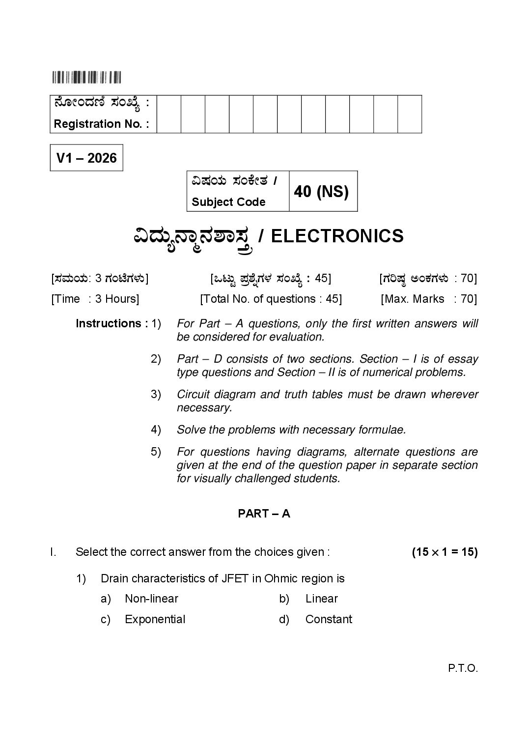
Registration No. :
V1 – 2026
«µÀAiÀÄ ¸ÀAPÉÃvÀ /
40 (NS)
Subject Code
«zÀÄå£Áä£À±Á¸ÀÛç / ELECTRONICS
[¸ÀªÀÄAiÀÄ: 3 UÀAmÉUÀ¼ÀÄ] [MlÄÖ ¥Àæ±ÉßUÀ¼À ¸ÀASÉå : 45] [UÀjµÀ× CAPÀUÀ¼ÀÄ : 70]
[Time : 3 Hours] [Total No. of questions : 45] [Max. Marks : 70]
Instructions : 1) For Part – A questions, only the first written answers will
be considered for evaluation.
2) Part – D consists of two sections. Section – I is of essay
type questions and Section – II is of numerical problems.
3) Circuit diagram and truth tables must be drawn wherever
necessary.
4) Solve the problems with necessary formulae.
5) For questions having diagrams, alternate questions are
given at the end of the question paper in separate section
for visually challenged students.
PART – A
I. Select the correct answer from the choices given : (15 × 1 = 15)
1) Drain characteristics of JFET in Ohmic region is
a) Non-linear b) Linear
c) Exponential d) Constant
P.T.O.
Page 2
2) For the faithful amplification the operating point is chosen at the
a) Center of the active region b) Cut off region
c) Saturation region d) Inversion region
3) Conduction angle for class-B power amplifier is
a) 60° b) 180°
c) 270° d) 360°
4) In a voltage series negative feedback amplifier
a) Input impedance increases b) Bandwidth decreases
c) Voltage gain increases d) Output impedance increases
5) Slew rate is expressed in
V μS
a) b)
μS V
A Ω
c) d)
mS mS
6) The feedback component used in Op-amp integrator circuit is
a) Resistor b) Diode
c) Transistor d) Capacitor
7) The crystal oscillator works on the principle of
a) Piezo magnetic effect b) Piezo static effect
c) Piezo electric effect d) Piezo dynamic effect
8) The medium through which the information flows is known as
a) Source b) Transmitter
c) Channel d) Receiver
Page 3
9) How many side bands are present in AM?
a) 1 b) 2
c) 3 d) 4
10) A SCR has
a) Two junctions and three layers
b) Three junctions and three layers
c) Three junctions and four layers
d) Four junctions and three layers
11) Logic expression for the output of two input XNOR gate is
a) Y = AB b) Y = A+B
c) Y = A d) Y = A⊕B
12) Group of two adjacent cells in a K-map is called
a) Pair b) Quad
c) Square d) Octet
13) The number of timers present in 8051 microcontroller is
a) One b) Two
c) Three d) Four
14) Size of an integer in C programming is
a) 1 byte b) 2 byte
c) 4 byte d) 8 byte
15) Expansion of CDMA is
a) Code Division Mobile Access
b) Call Division Mobile Access
c) Code Division Multiple Access
d) Call Division Multiple Access
Page 4
II. Fill in the blanks by choosing appropriate answer from the bracket : (5 × 1 = 5)
[ a) damped b) universal c) buffer d) timer e) demodulator f) summing ]
16) CC amplifier is used as _____________.
17) Op-amp inverting adder is also called as _____________ amplifier.
18) Tank circuit produces _____________ oscillations.
19) Diode detector is called as _____________.
20) NAND gate is also known as _____________ gate.
PART – B
III. Answer any five questions : (5 × 2 = 10)
21) Write the expressions for the coordinates of operating point in voltage
divider biasing circuit.
22) An amplifier has Z 0 = 50 kΩ , voltage gain A = 100 and β = 0.02 .
Determine the output impedance of the feedback amplifier.
23) A RC phase shift oscillator has R1 = R 2 = R 3 = R = 5 kΩ
and C1 = C2 = C3 = C = 0.022 μF . Calculate frequency of oscillations.
24) Write the expression for AM wave. Write the expression for ma in terms of
Vmax and Vmin .
25) List any four power devices.
26) Draw the logic circuit of a full adder using 3-input XOR gate.
27) Mention memory capacity of internal RAM and ROM of
8051 microcontroller.
28) Distinguish between uplink and downlink signals.
Page 5
PART – C
IV. Answer any five questions : (5 × 3 = 15)
29) Define drain resistance (rd ) , transconductance (g m ) and amplification
factor (μ ) in JFET.
30) Derive an expression for the voltage gain of a negative feedback
amplifier.
31) Sketch the nature of oscillator output waveform for a) Aβ > 1
b) Aβ < 1 and c) Aβ = 1.
32) Define critical angle, critical frequency and skip distance.
33) What are the characteristics of a good receiver?
34) Determine Vdc and Idc of SCR FWR. Given firing angle is 0° and rms
voltage of ac input to the rectifier is 230 V and load connected is 10Ω .
35) Convert Y = A + BC into canonical SOP form.
36) What is RADAR? Mention any two applications of RADAR.
PART – D (Section I)
V. Answer any three questions : (3 × 5 = 15)
37) Explain the working of transistor CB amplifier circuit.
38) What is an op-amp non inverting amplifier? Derive an expression for the
output voltage of op-amp non-inverting amplifier.
39) Why SR flip-flop is converted into D flip-flop? Explain the working of
D flip-flop with logic circuit and truth table.
40) Write ALP for multiplication of two unsigned 8-bit numbers 43H and
2 AH. Store the lower byte in R0 and higher byte in R1.
41) Write a C program to accept radius (in float) and print the area of the
circle.
Page 6
PART – D (Section II)
VI. Answer any two questions : (2 × 5 = 10)
42) For the CE amplifier circuit shown below :
Calculate
a) V2
b) IE
c) re′
d) AV
e) Zi (base )
26 mV
Given VBE = 0.7 V, re′ = , β = 100 .
IE
Page 7
43) Find the output voltage of Op-amp circuits given below :
a) (3)
b) (2)
44) The carrier current of AM transmitter is 12 A, it is increased to 13.25 A
when a carrier is amplitude modulated. Find the percentage modulation.
Determine antenna current It when the depth of modulation is 0.5 if
carrier current Ic remains at 12 A.
45) Simplify the Boolean expression
Y (A, B, C, D ) = m (2, 6, 7, 9, 12, 13 ) + d (3, 8 ) using K-map. Draw NAND
gate equivalent circuit to realize simplified equation.
Page 8
PART – E
(For Visually Challenged Students)
42) A single stage CE amplifier is provided with R1 = 90 kΩ , R 2 = 22 kΩ ,
26 mV
R C = 5 kΩ , RE = 1 kΩ , VCC = 12 V, VBE = 0.7 V , re′ = , β = 100 .
IE
Calculate
a) V2
b) IE
c) re′
d) A V and
e) Zi (base )
43) a) An op-amp subtractor circuit is given with V1 = 1 V, V2 = 2 V,
R f = 50 kΩ , R1 = 10 kΩ , R 2 = 10 kΩ and R 3 = 50 kΩ . Determine the
output voltage. (3)
b) An op-amp inverting amplifier circuit is given with Vin = 3 V,
R f = 20 kΩ and R i = 10 kΩ . Calculate the output voltage. (2)
—————
Document Details
| Board / Org | Karnataka Board |
| Exam | Class 12 |
| Type | Question Paper |
| Pages | 8 |
| Language | english |
| Updated | 24 Sep 2026 |